FPGA Setup for 100G Ethernet Data Logger
Using NVMe-IP for Gen5 Demo
1 Overview
This document provides a comprehensive guide for setting up an FPGA board to demonstrate the 100G Ethernet data logger using NVMe-IP for Gen5 demo. It includes step-by-step instructions for connecting an NVMe SSD to the FPGA board and linking the FPGA board to the network via 100G Ethernet to function as a 100G Ethernet data logger. Users will configure 100G Ethernet data logger parameters and monitor operations via a Nios terminal.
Packet filtering parameters are configured using “pkt_filter_cfg.exe”, a PC-based packet filtering configuration utility. This application assists users in converting standard Ethernet protocol fields and commonly used network parameters into the required Packet Filter configuration rules, which are then applied to the system.
2 Environment Requirements
Before running the 100G Ethernet data logger demo, ensure that the following hardware and software components are prepared and properly configured.
1) FPGA Development board: Agilex7 I-Series Development Kit.
2) PC Software
· Quartus Programmer for FPGA programming
· Nios Command Shell for user console
· Packet filtering configuration utility provided by Design Gateway: “pkt_filter_cfg.exe”
3) Micro-USB cable for FPGA programming and Nios Command Shell.
4) Two 100G Ethernet cables, connecting the FPGA to two Ethernet devices.
5) PCIe adapter board provided by Design Gateway
https://dgway.com/ABseries_E.html
· AB19-M2PCI: For M.2 SSD at CN#1
· AB20-U2PCI: For U.2 SSD at CN#1
6) NVMe Gen5 SSD connected via the PCIe adapter board.
7) Power adapter for the FPGA board.
8) ATX power supply for the PCIe adapter board.
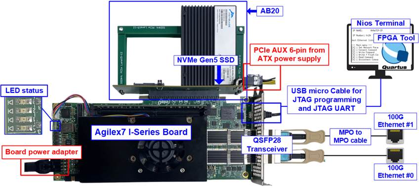
Figure 1 100G Ethernet Data Logger Demo on Agilex7 I-Series Board with AB20
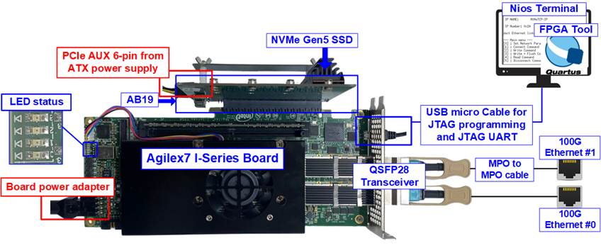
Figure 2 100G Ethernet Data Logger Demo on Agilex7 I-Series Board with AB19
3 Demo Setup
3.1 Hardware Setup
1) Ensure that the power switch is turned OFF before connecting the power supply to the FPGA board.
2) Connect a micro-USB cable from the FPGA board to the PC. This connection is used for JTAG programming and JTAG UART communication.
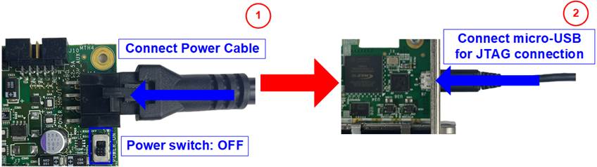
Figure 3 Power and micro-USB Connection
3) Establish the 100G Ethernet connections by inserting two 100G Ethernet cables into the FPGA board, connecting the FPGA board to two 100G Ethernet devices, as shown in Figure 4.
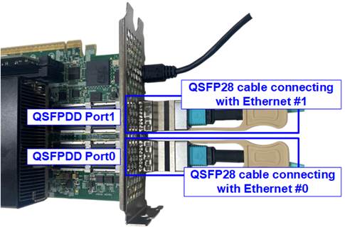
Figure 4 100G Ethernet Connection
4) Set SW2 bits[1:3] to OFF OFF OFF to support JTAG programming only, and SW3[3] to ON to select PCIe reference clock from PCIe connector.
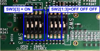
Figure 5 SW2 Setting on Agilex7 I-Series
5) Prepare the NVMe SSD and the NVMe adapter on your hardware configuration.
AB20-U2PCI
i) Ensure that two mini jumpers on JP1 of the AB20 board are inserted between pins 1-4 and 2-3.
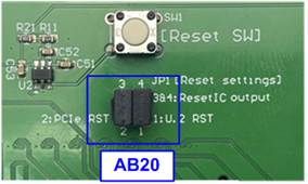
Figure 6 Jumpers on AB20
ii) Connect the NVMe SSD to CN1 (PCIe lane3-0) on the AB20 board.
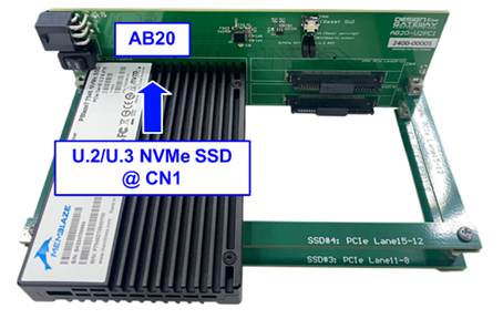
Figure 7 Connect U.2/U.3 NVMe SSD to CN1 of AB20
iii) Connect the 6-Pin PCIe AUX power cable from the ATX power supply to the AB20 board.
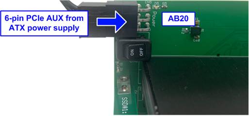
Figure 8 Connect PCIe AUX from Power Supply to AB20
iv) Adjust the height of the FPGA board to align with the PCIe connector on the AB20 board, and connect the AB20 to the FPGA board.
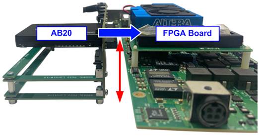
Figure 9 Adjust Height on FPGA Board and Connect AB20
AB19-M2PCI
i) Confirm that two mini jumpers are inserted at JP1, specifically between pins 1-3 and 2-4.
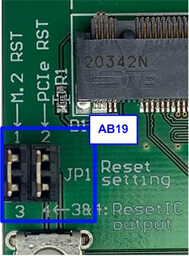
Figure 10 Jumper on AB19
ii) Connect the NVMe SSD to CN1 (PCIe lane3-0) on the AB19 board.
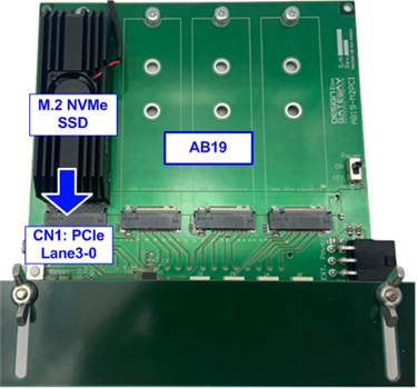
Figure 11 Connect NVMe SSD to AB19
iii) Connect the 6-Pin PCIe AUX from the ATX power supply to AB19 board as shown in Figure 12.
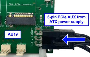
Figure 12 Connect 6-Pin PCIe Power Supply to AB19
iv) Insert AB19 board into the PCIe connector on the FPGA board.
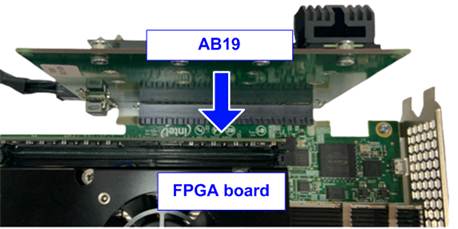
Figure 13 Connect AB19 to FPGA Board
v) Adjust the height of the AB19 by sliding the support board up or down until it is properly aligned with the PCIe connector on the FPGA board. Once aligned, tighten the wing nut to secure it in place.
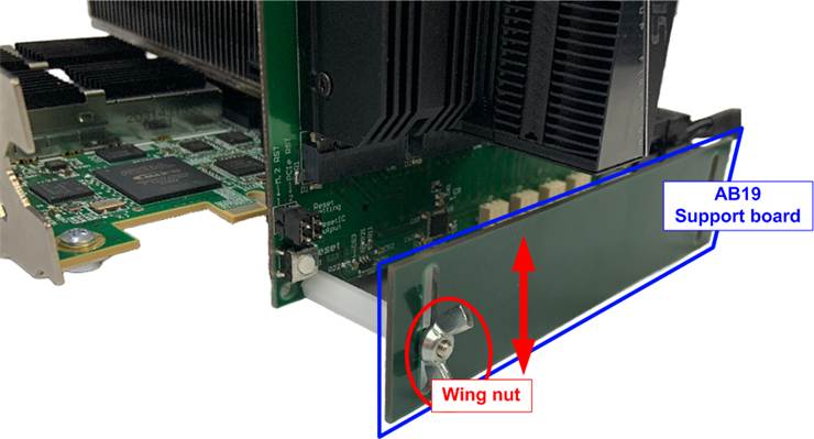
Figure 14 Adjust Height of AB19 Support Board
6) Power on the system.
i) Turn on ATX power supply connected to the NVMe adapter and turn on the power switch on the NVMe adapter.
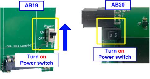
Figure 15 Power Switch on NVMe Adapter
ii) Turn on the power switch on the FPGA board.
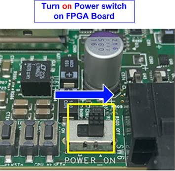
Figure 16 Power Switch on FPGA Board
7) Verify that the reference clock is correctly configured. For Agilex7 I-Series board, set the clock frequency of the Si5391 (OUT0) to 156.25 MHz.
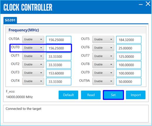
Figure 17 Set Clock Source on Agilex7 I-Series
3.2 File Programming
Follow these steps to program the demo file into the FPGA board.
1) Use Quartus Programmer to download the SOF file, as shown in Figure 18.
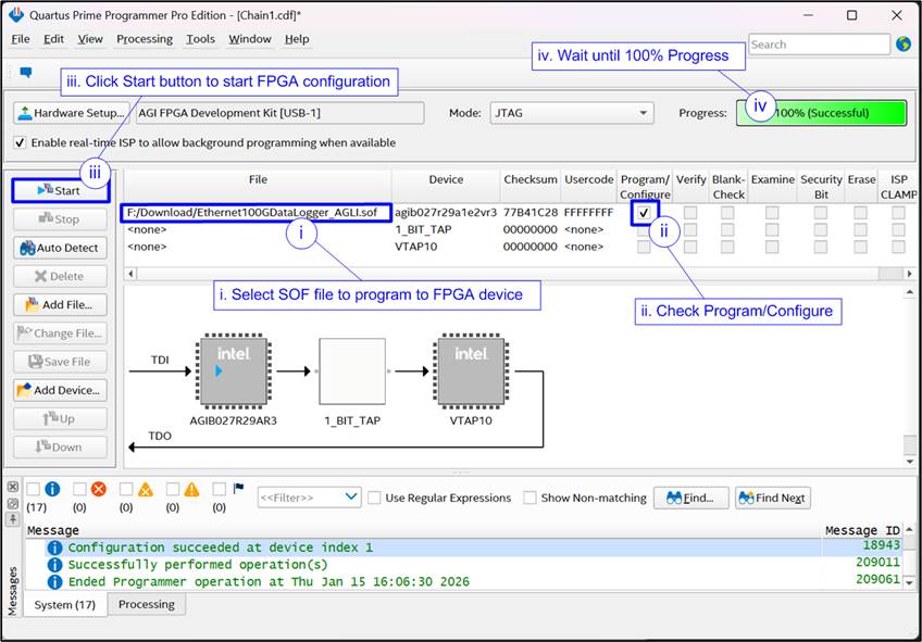
Figure 18 Programmed by Quartus Prime Programmer
2) Open the appropriate command shell on PC:
· For NiosII, open the Nios II Command Shell and run “nios2-terminal -d 1” to connect to the JTAG UART.
· For NiosV, open the Nios V Command Shell and run “juart-terminal -d 1” to connect to the JTAG UART.
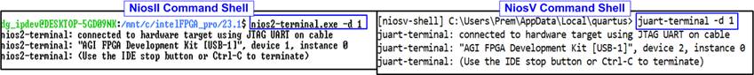
Figure 19 Open Nios Command Shell
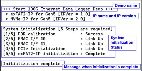
Figure 20 Nios Command Shell after FPGA is Completely Configured
3) After programming the FPGA, both LED[0] and LED[1] should be ON during initialization. Once the system completes initialization, LED[1] will turn OFF, as illustrated in Figure 21. For more information on LED behavior, refer to Table 1.
Table 1 LED Definitions
|
GPIO LED |
ON |
OFF |
|
0 |
Normal Operation |
Clock is not locked or reset button is pressed |
|
1 |
System is busy |
System is idle |
|
2 |
IP error detected |
Normal operation |
|
3 |
Forwarded Packet loss detected |
Normal operation |
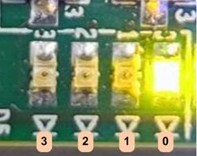
Figure 21 LED Status when the Initialization is Completed
4 Revision History
|
Revision |
Date (D-M-Y) |
Description |
|
1.00 |
4-Feb-26 |
Initial version release |