1. Introduction
AHCI (Advanced Host Controller Interface) is the standard to define behavior and software interface to communicate with Serial ATA devices. AHCI is a PCI class device that acts as a data movement engine between system memory and Serial ATA devices. More details about AHCI standard can be downloaded from below link.
http://www.intel.com/content/www/us/en/io/serial-ata/serial-ata-ahci-spec-rev1-3-1.html
This demo designs PCIe SSD by using AHCI-IP and SATA-IP from Design Gateway connecting with Xilinx AXI PCIe Bridge IP. AXI Interconnect is required to interface between AXI PCIe Bridge IP and AHCI-IP because of different clock domain and different data bus size, as shown in Figure 1‑1.

Figure 1‑1 PCIe AHCI-IP Demo System
This document does not describe the details about AHCI-IP block diagram and the operation. Please see AHCI-IP details from “SATA AHCI-IP reference design manual” document which can be downloaded from below link.
http://www.dgway.com/products/IP/SATA-IP/dg_sataahciip_refdesign_en.pdf
Comparing to SATA AHCI-IP reference design which is implemented on Zynq platfrom, the host controller is implemented by PC instead of ARM CPU. Since PC has greater CPU and RAM resource, PCIe AHCIP-IP can achieve better performance than Zynq platform. 4-lane PCIe Gen2 IP core which has 2000 MByte/sec bandwidth is selected for PC interface, so bandwidth is enough for SATA-III/II application. Two FPGA platforms are implemented for this demo, i.e. KC705 and VC707 board. PCIe physical connector on both FPGA boards is 8-lane, so Test PC must have available 8-lane Gen2 PCIe connector to run the demo.
2. Hardware
User interface of AXI PCIe Bridge is 128-bit AXI4 bus@125 MHz for both Master and Slave port to support 4-lane PCIe Gen2 speed. But SATA AHCI-IP needs to run at 150 MHz or higher clock frequency to interface with SATA-IP directly. So, AXI interconnect is required to support different clock domain between S_AXI of AXI PCIe Bridge and data bus of AHCI-IP. Also, the control register of AHCI-IP needs to run at 150 MHz or higher clock frequency and data bus size is only 32-bit interface. For control interface, AXI interconnect must be used to support both asynchronous clock and different bus size between M_AXI of AXI PCIe Bridge and register interface. AXIHBA block which is register interface of AHCI-IP can support only AXI4-Lite protocol, not AXI4, so data output of M_AXI must have only 1 DW size. Bigger size transfer from M_AXI will generate error condition in the system. More details about each block are described as follows.
2.1 AXI PCIe Bridge
In this demo, 100 MHz from PCIe connector is used to be reference clock. Physical setting of PCIe is 4-lane PCIe Gen2 speed to support SATA-III peripheral. Base class is set to be Mass storage controller and sub-class is set to be other mass storage controller to support AHCI feature with some special modification.
Note: Sub-class is set to other mass storage instead of AHCI to avoid the standard driver which may have already installed in TestPC. AHCI-IP has some modifications which are not compatible with standard driver.
128 KB register area within AHCI-IP is mapped to BAR0 address of PCIe. MSI Interrupt is enabled to support interrupt output signal from SATA AHCI-IP. In the demo, additional logic is designed to monitor that interrupt from SATA AHCI-IP is asserted more than 100 msec or not. If interrupt is asserted for long time, it will be expected that software may lose this interrupt. So, the logic will resend interrupt to AXI PCIe Bridge by re-generating new interrupt edge.
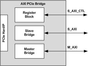
Figure 2‑1 AXI PCIe Bridge Block Diagram
As shown in Figure 2‑1, user interface of AXI PCIe Bridge has three buses, i.e. S_AXI_CTL for PCIe configuration access, S_AXI for receiving data request from AXI4 master, and M_AXI for sending data request to AXI4 slave. In the demo, S_AXI is used to DMA data transfer between main memory on PC and SATA-III/II device through AHCI-IP. Only data FIS type of SATA packet is transferred by this interface. Other FIS type of SATA packet is accessed by register interface through M_AXI bus like other AHCI control and status register. S_AXI_CTL is unused in the demo.
More details of AXI PCIe Bridge are described in “PG055 AXI Memory Mapped to PCI Express (PCIe) LogicCore IP Product Guide” document.
2.2 AXI HBA
This module is used to decode 128 KB BAR0 address from AXI PCIe Bridge and split into five areas, i.e.
- 0x0000_0000 – 0x0000_00FF : GHC Register
- 0x0000_0100 – 0x0000_017F : Port#0 Register
- 0x0000_8000 – 0x0000_80FF : Received FIS RAM (RxFisRAM)
- 0x0000_9000 – 0x0000_93FF : Command List RAM (CLstRAM)
- 0x0001_0000 – 0x0001_FFFF : Command Table RAM (CTblRAM)
GHC register is designed in HDL code while other registers/RAMs are implemented within AHCI-IP. More details about GHC register are described in topic 3.1 of “Serial SATA AHCI 1.3.1 Specification” document.
2.3 SATA AHCI-IP and SATA-IP
Please see more details from IP datasheet and reference design document.
3. Software
This topic lists the modification point of driver in the demo from the standard driver.
1) Following AHCI standard, BAR5 address is used to map GHC and Port#0 register. But AXI Bridge IP can support up to three BAR addresses (BAR0 – BAR2). Hardware in the demo needs to use BAR0 area instead of BAR5. So, driver is modified to use BAR0 address following the hardware design.
2) Extend BAR0 area to be 128 Kbyte to map Received FIS RAM, Command List RAM, and Command Table RAM to BAR0 area instead of main memory.
3) Set total port number of AHCI to be 1 port instead of 32 ports. In the demo, only one SATA-III/II device can be connected.
4) Set total number of PRD entries to 120 which is the limitation from RAM size in AHCI-IP. Default value in driver is 168.
5) Change function to assign value to Command List and Command Table from passing value by using pointer to be writel function instead for hardware register access.
4. Revision History
|
Revision |
Date |
Description |
|
1.0 |
14-Jul-15 |
Initial Release |
|
|
|
|
Copyright: 2015 Design Gateway Co,Ltd.