SATA HCTL IP Core Data Sheet

Core Facts |
|
|
Provided with Core |
|
|
Documentation |
User Guide, Design Guide |
|
Design File Formats |
Encrypted Netlist File |
|
Constraints Files |
User constraint file |
|
Instantiation Templates |
VHDL |
|
Reference Designs & Application Notes |
Vivado Project, See Reference Design Manual |
|
Additional Items |
Demo on AC701/KC705/ ZC706/VC707/VC709/KCU105/ Zynq Mini-ITX/ZCU102/VCU118 |
|
Support |
|
|
Support Provided by Design Gateway Co., Ltd. |
|
Design Gateway Co.,Ltd
54 BB Building 14th Fl., Room No.1402 Sukhumvit 21 Rd. (Asoke), Klongtoey-Nua, Wattana, Bangkok 10110
Phone: 66(0)2-261-2277
Fax: 66(0)2-261-2290
E-mail: ip-sales@design-gateway.com
URL: www.design-gateway.com
Features
· Simple user interface by dgIF typeS
· Pin compatible to DG SATA-IP
· Small logic resource without BlockRAM utilization
· Suitable for system without CPU and external memory (DDR)
· Support four ATA commands for application layer, i.e. IDENTIFY DEVICE, SECURITY ERASE UNIT, WRITE DMA (EXT), and READ DMA (EXT)
· Reference design with DG SATA-IP by using AB09-FMCRAID adapter board on AC701/KC705/ ZC706/VC707/VC709/KCU105/Zynq Mini-ITX/ZCU102/VCU118 board
Table 1: Example Implementation Statistics for Ultrascale device
|
Family |
Example Device |
Fmax (MHz) |
CLB Regs |
CLB LUTs |
CLB1 |
IOB |
BUFG |
RAMB18 |
PLL |
GTH/GTY |
Design Tools |
|
Kintex-Ultrascale |
XCKU040FFVA1156-2E |
476 |
563 |
704 |
161 |
- |
- |
- |
- |
- |
Vivado2015.4 |
|
Zynq-Ultrascale+ |
XCZU9EG-FFVB1156-2-I |
>500 |
559 |
473 |
135 |
- |
- |
- |
- |
- |
Vivado2017.3 |
|
Vertex-Ultrascale+ |
XCVU9P-FLGA2104-2L-E |
>600 |
579 |
671 |
145 |
- |
- |
- |
- |
- |
Vivado2017.4 |
Notes:
1) Actual slice count dependent on percentage of unrelated logic. The example is the report from utilization_placed.rpt file.
2) Assuming clocks are routed off-chip
Table 2: Example Implementation Statistics for 7-Series device
|
Family |
Example Device |
Fmax (MHz) |
Slice Regs |
Slice LUTs |
Slices1 |
IOB |
BUFG |
RAMB18 |
PLL |
GTP/GTX |
Design Tools |
|
Artix-7 |
XC7A200TFBG676-2 |
263 |
563 |
578 |
238 |
- |
- |
- |
- |
- |
Vivado2015.4 |
|
Kintex-7 |
XC7K325TFFG900-2 |
370 |
563 |
704 |
278 |
- |
- |
- |
- |
- |
Vivado2015.4 |
|
Zynq-7000 |
XC7Z045FFG900-2 |
400 |
563 |
708 |
275 |
- |
- |
- |
- |
- |
Vivado2015.4 |
|
Virtex-7 |
XC7VX485TFFG1761-2 |
357 |
563 |
703 |
271 |
- |
- |
- |
- |
- |
Vivado2015.4 |
Notes:
1) Actual slice count dependent on percentage of unrelated logic. The example is the report from utilization_placed.rpt file.
2) Assuming clocks are routed off-chip
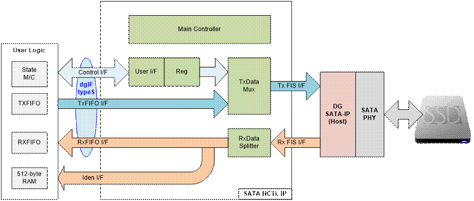
Figure 1: SATA HCTL IP block Diagram
Applications
SATA HCTL IP Core operating with DG SATA-IP and SATA PHY is ideal to access SATA device without using both CPU and external memory. The resource utilization of the IP is less, but it can achieve very high performance. Using multiple IPs as RAID0 increases total performance of storage system. So, it is recommended to use the IP in very high-speed data recording system or big-data storage.
General Description
SATA HCTL IP Core implements the application layer and remaining part of transport layer which is not implemented in DG SATA-IP. So, it is easy for user to write/read data with SATA device by designing the logic to interface SATA HCTL IP through dgIF typeS interface. dgIF typeS interface is DG interface standard for all storage IPs. dgIF typeS interface consists of command interface and data interface. Command interface signals are command value, start address, and transfer length for command interface. Data interface signals are same as general FIFO interface. Four ATA commands are supported, i.e. IDENTIFY DEVICE to check SATA device capacity, SECURITY ERASE UNIT to erase data in SATA device, WRITE DMA (EXT) to write data to SATA device, and READ DMA (EXT) to read data back from SATA device. Clock domain for SATA HCTL IP must be same as user clock of DG SATA-IP because there is no asynchronous circuit inside SATA HCTL IP. Error signal will be asserted if the FIS packet sequence is not correct.
The reference design to test write/read data with SATA-II/III device on Xilinx evaluation board are available to download for evaluation before purchasing.
Functional Description
Command Processor
After system power-on, HCTL IP waits Signature FIS returned from SATA device to complete initialization process. After that, the IP is ready to receive new command from user. When user sends command request to HCTL IP, the IP creates Command FIS from user parameters and forwards to SATA-IP. If total transfer size is more than maximum size in one command (32 MB), the IP will create multiple commands to SATA-IP until total size is equal to set value from user.
· User I/F and Reg
Command, Address, and transfer size from user request are latched into the register. Internal logic builds Command FIS from the parameter. Four commands are supported, i.e. Identify Device, Security Erase, Write, or Read command.
· Main Controller
Control FIS packet sequence for each command and select data source to transmit to SATA-IP. Data source is TXFIFO to transmit Data FIS to SATA-IP while data source is User I/F and Reg to transmit non Data FIS to SATA-IP. Otherwise, status packet which is returned from SATA device is monitored by Main controller to confirm that the command is processed completely.
Data Processor
To create Data FIS in Write command, data from TxFIFO is combined with the header which is inserted by internal logic to build SATA FIS packet. If transfer data size is more than one FIS packet size, data stream from TxFIFO will be split to many packets before forwarding to SATA-IP. For Read command, the header in Data FIS packet is removed and raw data without the header is forwarded to RxFIFO interface. Data output from Identify device command is transferred to Iden I/F, not RxFIFO I/F.
· TxData Mux
Data Multiplexer selects data source to build SATA FIS packet following the control signal from Main Controller. Transmit packet could be Command FIS from User I/F and Reg or Data FIS from TXFIFO.
· RxData Splitter
Received FIS returned from SATA-IP is decoded to check FIS type. In Read command, Data FIS without the header is stored to RxFIFO I/F. In Identify device command, Data FIS without the header is forwarded to Iden I/F. For other FIS types, the packet is decoded and monitored by Main Controller to check that the operation of each command is completed without the error.
User Logic
This block can be designed by using simple logic. Figure 1 shows the example of user logic which consists of State machine and two FIFOs. State machine is designed to create parameters of Control I/F and monitors status of Control I/F. Two FIFOs are applied to connect with Data I/F of SATA HCTL IP. To store data from Identify device command, 512-byte RAM could be applied.
DG SATA-IP
DG SATA-IP implements Transport layer and link layer of SATA protocol. It supports to run in Host or Device mode. To connect with SATA HCTL IP, SATA-IP runs in Host mode. More details of DG SATA-IP are described in the datasheet as following link.
http://www.dgway.com/products/IP/SATA-IP/dg_sata_ip_data_sheet_7series_en.pdf
SATA PHY
SATA PHY implements Physical layer of SATA protocol. It consists of the logic for controlling SATA signal initialization sequence and FPGA transceiver for converting data bus to Serial interface. The characteristic and the parameter of FPGA transceiver is different in each FPGA model. So, the reference design of SATA HCTL IP uses different SATA PHY for each FPGA model.
Core I/O Signals
Descriptions of all signal I/O are provided in Table 3.
Table 3: Core I/O Signals
|
Signal |
Dir |
Description |
|
dgIF typeS |
||
|
RstB |
In |
Synchronous reset signal. Active low. Release to ‘1’ after Clk signal input is stable. |
|
Clk |
In |
Clock for running HCTL IP. Must use the same clock as trn_clk of SATA-IP. (At least 150 MHz for SATA3 operation or at least 75 MHz for SATA2 operation) |
|
UserCmd[1:0] |
In |
User Command. “00”: Identify device command, “01”: Security erase unit command, “10”: Write SATA device, “11”: Read SATA device. Note: 1) Security erase unit operation time depends on SATA device characteristic. It may take long time to complete the operation. So, timeout counter in IP will be disabled in Security erase unit command. 2) Security erase unit is not mandatory command, so user should check SATA device specification firstly that the device can support this command before using it. |
|
UserAddr[47:0] |
In |
Start address of SATA device to write/read in sector unit (512 byte). |
|
UserLen[47:0] |
In |
Total transfer size in the request. Must not set equal to 0. Valid from 1 to (LBASize-UserAddr). |
|
UserReq |
In |
Request the new command. Can be asserted only when the IP is Idle (UserBusy=’0’). Asserted with valid value on UserCmd/UserAddr/UserLen signals. |
|
UserBusy |
Out |
IP Busy status. New request will not be allowed if this signal is asserted to ‘1’. |
|
LBASize[47:0] |
Out |
Total SATA device capacity in sector unit (512 byte). Default value is 0. This value is updated after user sends Identify device command. |
|
UserError |
Out |
Error flag. Assert to ‘1’ when UserErrorType is not equal to 0. The flag can be reset only by asserting RstB signal. |
|
UserErrorType[31:0] |
Out |
Error status. Details of the error flag is as follows. [0] – Error from SATA-IP such as CRC error, wrong primitives sequence. [1] – Error from Data FIS header [2] – Error from returned Status FIS [3] – Error from DMA active FIS. Write operation cannot complete. [4] – Error from PIO Setup FIS. Failure during SATA device identification process. [5] – Timeout error. No FIS returned from SATA device in time. [31:6] - Reserved |
|
UserFifoWrCnt[15:0] |
In |
Write data counter of received FIFO. Used to check full status. If total FIFO size is less than 16-bit, please fill ‘1’ to upper bit. UserFifoWrEn can be asserted to ‘1’ when UserFifoWrCnt[15:3] is not equal to all 1. |
|
UserFifoWrEn |
Out |
Write data valid of received FIFO. |
|
UserFifoWrData[31:0] |
Out |
Write data bus of received FIFO. Synchronous to UserFifoWrEn. |
|
UserFifoRdCnt[15:0] |
In |
This signal is unused for this IP. |
|
UserFifoEmpty |
In |
FIFO empty flag of transmit FIFO to check data available status. |
|
UserFifoRdEn |
Out |
Read valid of transmit FIFO. |
|
UserFifoRdData[31:0] |
In |
Read data returned from transmit FIFO. Valid in the next clock after UserFifoRdEn is asserted to ‘1’. |
|
Signal |
Dir |
Description |
|
HCTL IP Interface |
||
|
TestPin[31:0] |
Out |
Reserved to be IP test point. |
|
TimeOutSet[31:0] |
Out |
Timeout value to wait FIS returned from SATA device. Time unit is equal to the period of Clk signal. |
|
IdenWrEn |
Out |
Valid signal of IdenWrAddr and IdenWrData. Asserted to ‘1’ after Identify Device command is requested. |
|
IdenWrAddr[6:0] |
Out |
Index of IdenWrData in 32-bit unit. Synchronous to IdenWrEn |
|
IdenWrData[31:0] |
Out |
512-byte data from Identify device command. Synchronous to IdenWrEn. |
|
SATA-IP Interface (Host) |
||
|
trn_rd[31:0] |
In |
Receive data bus from SATA-IP. |
|
trn_rsof_n |
In |
Receive start-of-frame. Indicates start of SATA FIS packet. Active low. |
|
trn_reof_n |
In |
Receive end-of-frame. Indicates end of SATA FIS packet. Active low. |
|
trn_rsrc_rdy_n |
In |
Receive source ready. Indicates that trn_rd is valid. Active low. |
|
trn_rsrc_dsc_n |
In |
Receive disconnect from SATA-IP. Active low. |
|
trn_rdst_rdy_n |
Out |
Receive ready. Indicate that the IP is ready to accept data. Active low. |
|
trn_rdst_dsc_n |
Out |
Receive disconnect from the IP. Active low. This value is always set to ‘1’. |
|
trn_td[31:0] |
Out |
Transmit data bus to SATA-IP. |
|
trn_teof_n |
Out |
Transmit end-of-frame. Indicates end of SATA FIS packet. Active low. |
|
trn_tsrc_rdy_n |
Out |
Transmit source ready. Indicates that trn_td is valid. Active low. |
|
trn_tsrc_dsc_n |
Out |
Transmit abort from the IP. Active low. This value is always set to ‘1’. |
|
trn_tdst_rdy_n |
In |
Transmit ready. Indicates that SATA-IP is ready to accept data. Active low. |
|
trn_tdst_dsc_n |
In |
Transmit abort from SATA-IP. Active low. |
Timing Diagram
Initialization
The sequence of the initialization process is as follows.
1) RstB is released to ‘0’ by user after Clk is stable. UserBusy is asserted to ‘1’.
2) HCTL-IP waits until Signature FIS returned from SATA device. Next, UserBusy is de-asserted to ‘0’.
After complete above sequence, HCTL-IP is ready to receive the command from user.
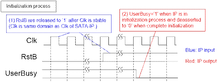
Figure 2: RstB and UserBusy during IP intialization
dgIF typeS
dgIF typeS signal is split into two interfaces, i.e. command interface and data interface. Figure 3 shows timing diagram of command interface of dgIF typeS. Before sending new command to the IP, UserBusy must be monitored to confirm that IP is Idle. UserCmd, UserAddr, and UserLen must be valid and latched during asserting UserReq=’1’. UserBusy changes from ‘0’ to ‘1’ after starting new command operation. Finally, UserReq is de-asserted to ‘0’ and user logic can prepare the next command to the command bus.
Note: UserAddr and UserLen value are ignored in Identify device command and Security erase command.
For data interface, Transmit FIFO is read for Write command, while Received FIFO is written for Read command. Timing diagram of data interface is shown in Figure 4 and Figure 5.
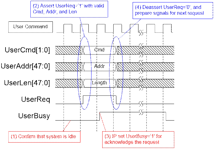
Figure 3: Command interface of dgIF typeS timing diagram
For Write command, UserFifoEmpty is monitored to wait data available in Transmit FIFO. When Transmit FIFO has data (UserFifoEmpty=’0’), UserFifoRdEn is asserted to ‘1’ and data from Transmit FIFO (UserFifoRdData) is valid in the next clock. UserFifoRdEn is asserted to ‘1’ until total data are transferred (Total data=UserLen) or FIFO is empty, as shown in Figure 4.
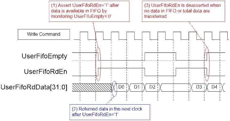
Figure 4: Transmit FIFO interface for Write command
For Read command, UserFifoWrEn is asserted with the valid UserFifoWrData. UserFifoWrCnt is monitored to check that free space in the FIFO is more than 7 (UserFifoWrCnt < 65528 or 0xFFF8). If free space is less than 7, UserFifoWrEn will be deasserted to ‘0’ to pause data transferring.
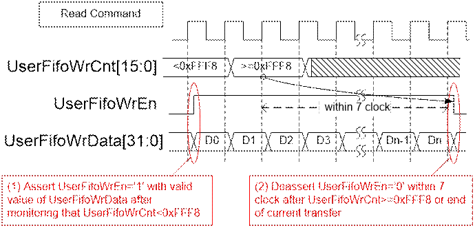
Figure 5: Received FIFO interface for Read command
Identify Device
The first command sending to IP must be Identify device command for updating LBASize signal. LBASize is used in User Logic to check that the sum of address and length in Write/Read command is not out-of-range. All 512-byte data from Identify device command is sent to Iden I/F. User can decode SATA device information such as model number, supported feature from Identfiy device data.
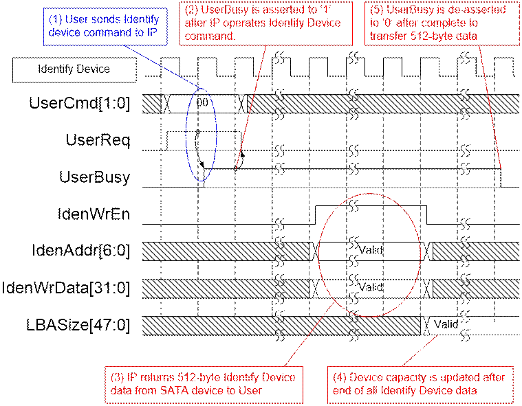
Figure 6: LBASize is updated after Identify device command
Security Erase Unit
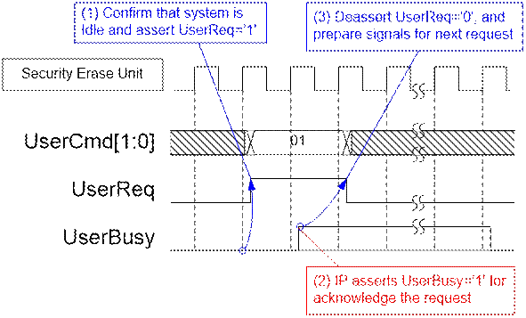
Figure 7: User interface in Security Erase Unit command
Similar to Identify device command, UserAddr and UserLen input are not used for Security Erase Unit command. User should confirm from SATA device specification or from Identify device data firstly that the device can support this command. Erase time of each device is different and may be rather long in some devices. User can check the estimation erase time from Identify device data. UserBusy is asserted to ‘1’ until the device complete erase operation.
Error
During normal operation, UserError and all bits of UserErrorType signal are always 0. UserError is generated by OR condition of each-bit of UserErrorType. If some bit of UserErrorType is set to ‘1’, UserError is asserted and latched until RstB is asserted to ‘0’, as shown in Figure 8.
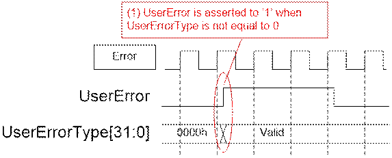
Figure 8: Error flag timing diagram
Verification Methods
The SATA HCTL IP Core functionality was verified by simulation and also proved on real board design by using AC701/KC705/ZC706/VC707/VC709/KCU105/Zynq Mini-ITX/ZCU102/VCU118 evaluation board.
Recommended Design Experience
Experience design engineers with a knowledge of Vivado Tools should easily integrate this IP into their design.
Ordering Information
This product is available directly from Design Gateway Co., Ltd. Please contact Design Gatway Co., Ltd. For pricing and additional information about this product using the contact information on the front page of this datasheet.
Revision History
|
Revision |
Date |
Description |
|
1.0 |
Oct-9-2014 |
New release |
|
1.1 |
Aug-29-2016 |
Update I/O signal and support Kintex Ultrascale device |
|
1.2 |
Nov-9-2016 |
Add security erase command and support Mini-ITX/VC709 board |
|
1.3 |
Jan-30-2017 |
Update interface to dgIF typeS |
|
1.4 |
Jan-9-2018 |
Support ZCU102 board |
|
1.5 |
May-4-2018 |
Support VCU118 board |