SATA-IP Bridge reference design on KC705 manual
Rev1.1 23-Aug-23
1. Introduction
Serial ATA (SATA) is an evolutionary replacement for the Parallel ATA (PATA) physical storage interface. SATA interface increases speed transfer to be 3.0 Gbps for SATA-II and 6.0 Gbps for SATA-III. To communication by SATA protocol, there are four layers in its architecture, i.e., Application, Transport, Link, and Phy.
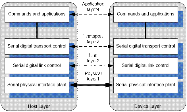
Figure 1 SATA Communication Layer
The Application layer is responsible for overall ATA command execution, including controlling Command Block Register accessed. The Transport layer is responsible for placing control information and data to be transferred between the host and device in a packet/frame, known as a Frame Information Structure (FIS). The Link layer is responsible for taking data from the constructed frames, encoding or decoding each byte using 8b/10b, and inserting control characters such that the 10-bit stream of data may be decoded correctly. The Physical layer is responsible for transmitting and receiving the encoded information as a serial data stream on the wire.
This reference design provides evaluation system which implements all SATA communication layers for Host and Device side to demonstrate SATA Bridge operation at SATA-III speed. The SATA-IP core is designed to operate with GTX transceiver of the Kintex-7 platform in the reference design on KC705 Evaluation board. More details are described as follows.
2. Environment
This reference design is based on the following environment as shown in Figure2.
l KC705 Platform
l Vivado 2019.1
l AB09-FMCRAID board, provided by Design Gateway
l AB02-CROSSOVER board, provided by Design Gateway
l 2.5-inch SATA cable connecting to CN0 connector on FMCRAID board and SATA-III PC
l SATA-III Device (HDD/SSD) connecting to CN1 connector on FMCRAID board
l USB Micro-B cable for FPGA configuration
l USB Mini-B cable for serial communication. For serial communication, set baud rate=115,200 / data=8bit / Non-Parity / Stop=1bit.
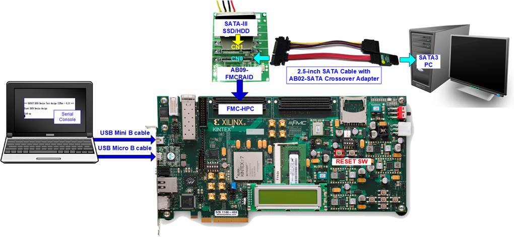
Figure 2 Reference design environment
More details to show step-by-step to run the demo on real test environment, please refer to “SATA-IP Bridge Demo Instruction on KC705” document.
3. Hardware description
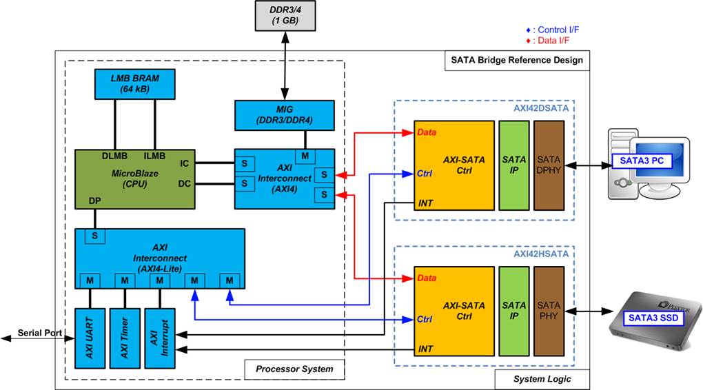
Figure 3 Block diagram of the reference design
l SATA IP Bridge design implementation on Kintex7 FPGA
As shown in Figure 3, the demo system consists of three parts. First is Processor system which consists of the processor and its peripherals. Second is AXI42DSATA module which is hardware logic for interface with SATA host (PC). Third is AXI42HSATA module which is hardware logic for interface with SATA device (HDD/SSD).
Processor system includes the basic components such as UART, Timer, Interrupt controller, DDR controller, and Block RAM for storing instruction/data of the processor. AXI4-Lite and AXI4 interface in Processor system are exported to connect the hardware logic on top level.
AXI4-Lite bus is the simple interface for memory access by single access. Therefore, it is applied to connect to slow-speed CPU peripherals. The control and status registers of AXI42HSATA and AXI42DSATA are connected to the processor by using this bus. While AXI4 bus is more complicate interface that transfers the data as burst mode for high-speed CPU peripherals such as DDR memory. AXI42HSATA and AXI42DSATA transfer the data with DDR memory by using AXI4 bus in master mode to achieve high-speed performance. Therefore, AXI4-Lite and AXI4 interface are exported from processor system to connect to AXI42HSATA and AXI42DSATA in HDL code of System logic which is the top module. The details of SATA-IP device demo are described as follows.
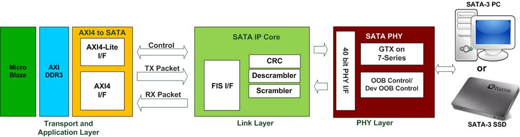
Figure 4 AXI-SATACtrl Block Diagram
l PHY Layer
This layer is designed by using GTX module (built-in high speed serial circuit) of Kintex-7 device, operating with logic control to generate OOB sequence and initialization sequence of physical layer. There are two different PHY designs to operate Host and Device mode.
For host mode, state machine to control OOB is designed in “oob_control.vhd” which is sub-module of “sata2phy_k7.vhd”, the top layer of PHY source code which also includes Xilinx transceiver module and the interface logic.
For device mode, OOB sequence in “dev_oob_control.vhd” is reversed to host mode operation. Similar to host mode, the top module, “sata2dphy_k7.vhd”, includes OOB module and transceiver parameter setting.
PHY design in reference design follows PLL and GTX reset sequence described in “7 Series FPGAs GTX/GTH Transceivers” user guide, refer to “Reset and Initialization” section in ug476 for detailed reset sequence. Before building user board, user must read carefully and must follow design guide line described in UG476 (7 Series FPGAs GTX/GTH Transceivers User Guide).
l Link Layer by SATA-IP
Link Layer and some part of Transport layer are implemented by SATA-IP. FIS packet format is converted to lower-layer protocol by CRC calculating and scramble processing. Also, low-level packet from physical layer is decoded and arranged to FIS packet format for interface with user. The host and device operation in this module are similar. More details about SATA-IP interface are described in “dg_sata_ip_datasheet_kt7_en” document.
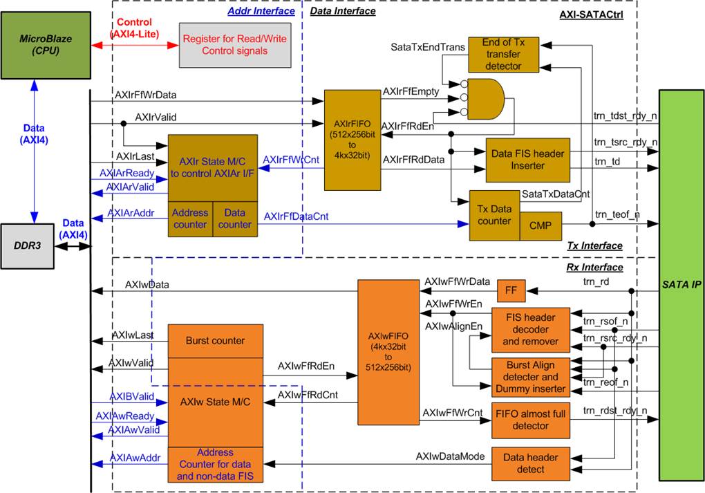
Figure 5 Block diagram of AXI-SATACtrl
l Transport Layer by AXI-SATACtrl
For this layer, the host and device mode use the same design structure, but connecting to different PHY module. The details of the module are follows.
AXI-SATACtrl is the logic design to connect SATA-IP interface to standard interface within Processor system, i.e., AXI4-Lite interface for control signal and AXI4 for data signal. AXI4-Lite interface connects to MicroBlaze while AXI4 interface running as master mode connects to DDR3 controller.
|
Address |
Register Name |
Description |
|
Rd/Wr |
(Label in the “sata_bridge.c” ) |
|
|
BA+0x04 |
Error Code Reg. |
SATA IP Error code after transmit/receive completion to detect CRC or FIS error. |
|
Rd |
(ERROR_CODE) |
|
|
BA+0x0C |
Receive Word Count Reg. |
[31] : Received FIS type in this interrupt (‘1’: Non-Data FIS, ‘0’: Data FIS). This bit is cleared by writing bit[29] of INT_CLEAR = ‘1’. [23:0] : Total received word count of FIS data. Auto clear when next transfer start (CONTROL Reg is written). |
|
Rd |
(RX_COUNT) |
|
|
BA+0x10 |
SATA-IP Version |
[31:0] Version number of SATA-IP |
|
Rd |
(IPVERSION) |
|
|
BA+0x00 |
Transmit Data Address Reg. |
Set DDR3 start address of transmit FIS data area Bit[8:0] of this value needs to be equal to 0 for sector alignment. |
|
Wr |
(TX_ADDR) |
|
|
BA+0x04 |
Received Data Address1 Reg. |
Set DDR3 start address of other received FIS area (except DATA FIS type). Bit[8:0] of this value needs to be equal to 0 for sector alignment. |
|
Wr |
(RX_ADDR) |
|
|
BA+0x08 |
Control Reg. |
[31] : Assert to ‘1’ for hardware Reset [30] : Assert to ‘1’ to start transmitting data [29] : FIS type (‘1’: Data, ‘0’: Others) [15:0] : Total Transmit word count. RX_COUNT register is cleared by write operation to this register |
|
Wr |
(CONTROL) |
|
|
BA+0x0C |
Received Data Address2 Reg. |
Set DDR3 start address of received DATA FIS area Bit[8:0] of this value needs to be equal to 0. |
|
Wr |
(RX2_ADDR) |
|
|
BA+0x10 |
Interrupt Clear Reg |
[31] : Assert to ‘1’ to clear ip2host interrupt [30] : Assert to ‘1’ to clear host2ip interrupt [29] : Assert to ‘1’ to clear received FIS type |
|
Wr |
(INT_CLEAR) |
Table 1 Register mapping from CPU side
(BA : Base Address for Host is 0x4800_0000 and Base Address for Device is 0x4801_0000)
Register map of control signals to interface with MicroBlaze by AXI4-Lite bus is shown in Table 1. Main operations of these registers are to define DDR address for transferring FIS data, transfer length, and FIS type (data or non-data). Also, the status of operation can be monitored by MicroBlaze when accessing these registers.
For transferring data with DDR3, it uses AXI4 bus interface. AXI4 bus can be divided into four groups, i.e., AXIAr for read command request, AXIr for read data transferring, AXIAw for write command request, and AXIw for write data transferring. The requests for both read and write command are controlled by state machine. Data bus size of AXI4 is 256-bit, so the FIFO must be used for data bus converting between 256-bit and 32-bit (SATA-IP bus size). The sequence of read and write operation are as follows.
For read operation from AXI to SATA, the operation is started by MicroBlaze. After FIS or data is prepared in DDR3, MicroBlaze sets CONTROL register to start transferring data or non-data FIS to SATA with setting the packet size. If data FIS is sent, Data FIS header will be auto-added by internal logic and then followed by the data from DDR3. AXIrFIFO is applied to convert data bus size and for data flow control. If FIFO is almost full, state machine will pause the next data request from DDR to wait until FIFO free space is enough. Also, the logic at SATA side monitors empty flag of FIFO to start reading and forwarding to SATA-IP when FIFO is not empty.
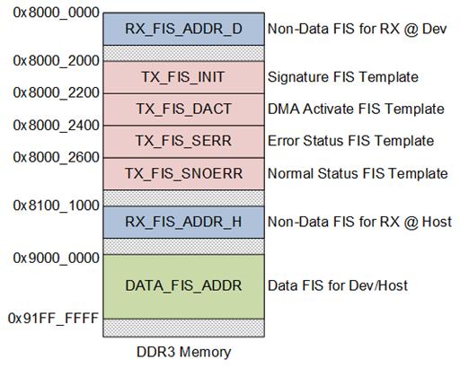
Figure 6 DDR3 Memory map in the demo
For write operation from SATA to AXI, the operation is started by SATA. Some areas of DDR3 are applied to store the FIS template prepared by MicroBlaze to return to PC for SATA device operation, i.e., TX_FIS_INIT, TX_FIS_DACT, TX_FIS_SERR, and TX_FIS_SNOERR. Also, DDR3 areas stores Data FIS and non-DATA FIS packet at different area, as shown in Figure 6. Data FIS is stored to DATA_FIS_ADDR area while non-DATA FIS is stored to RX_FIS_ADDR_D/H following the operation mode. AXIwFIFO is used for data flow controlling and data bus size converting. If AXIwFIFO is almost full, SATA packet from SATA-IP will pause data transferring. Also, when SATA packet size received from SATA-IP is too small and not aligned word (less than 256-bit), the dummy word is filled to FIFO by internal logic to align 256-bit size. At the read side of AXIwFIFO, state machine always monitors FIFO count to check if the data is much enough. Next, the write request is asserted and the data is forwarded to DDR3 through AXI4 bus. The FIS header of every SATA packet is decoded to check FIS type that is non-data or data type to select DDR3 address area for storing FIS packet
Data burst size in both directions are fixed to 256-bitx16 beat (512 byte) for simple design logic and high-speed transferring. AXI-SATACtrl logic operating with SATA-IP and PHY layer code are stored in “AXI42HSATA.vhd” for host mode and “AXI42DSATA.vhd” for device mode, provided to user as delivery item.
4. Software description
l SATA Bridge operation
SATA Bridge firmware is modified from SATA Device and SATA Host demo reference design. Unlike both host and device designs, SATA FIS (Frame Information Structure) is typically not created by MicroBlaze, but MicroBlaze is only forwarded SATA FIS from Host to Device or Device to Host. However, the FIS is still decoded by MicroBlaze before forwarding for analyzing the command sequence and controlling data flow to the main memory by DMA controller within both host and device designs.
MicroBlaze in the SATA Bridge operates as below sequence.
(1) Receive FIS Data (command) from PC
(2) Decode and execute the ATA command
(3) Forward FIS Data (command) to HDD/SSD
(4) Forward additional FIS data if necessary (for data command)
(5) Wait FIS Data (status) returned from HDD/SSD
(6) Forward FIS Data (status) to PC
l Software of reference design
Software source code of Bridge reference design is stored in “sata_bridge.c”. For simple design, the demo does not support some features, i.e.,
- TRIM
- NCQ (Native Command Queuing)
- More than 1 sector PIO Read and Write command
Typically, MicroBlaze forwards FIS Data from one side to another side except READ DMA (EXT) and WRITE DMA (EXT) command which needs to optimize data sequence to achieve high performance.
l READ DMA (EXT)
The brief sequence of bridge firmware is follows.
(1) Decode total data size from Command FIS.
(2) Forward Command FIS from the device mode (connecting to PC) to the host mode (connecting to HDD/SSD).
(3) Wait data returned from HDD/SSD.
(4) If data is enough, MicroBlaze will set register at device side (PC) to send FIS Data from DDR3.
(5) Step (3) – (4) are repeated until finishing transferring all data.
(6) Wait FIS Data (status) returned from HDD/SSD.
(7) Forward FIS Data (status) to PC.
l WRITE DMA (EXT)
The brief sequence of bridge firmware is follows.
(1) Decode total data size from Command FIS.
(2) Create and Send DMA Activate FIS to the device mode (PC).
(3) Wait data from PC.
(4) Forward data to the host side (HDD/SSD) when data is enough and DMA Activate FIS is received from HDD/SSD.
(5) Step (3) – (4) are repeated until finishing transferring all data.
(6) Wait FIS Data (status) from HDD/SSD.
(7) Forward FIS Data (status) to PC
l Performance result
Figure 7 shows the example performance when running disk benchmark through SATA Bridge reference design.
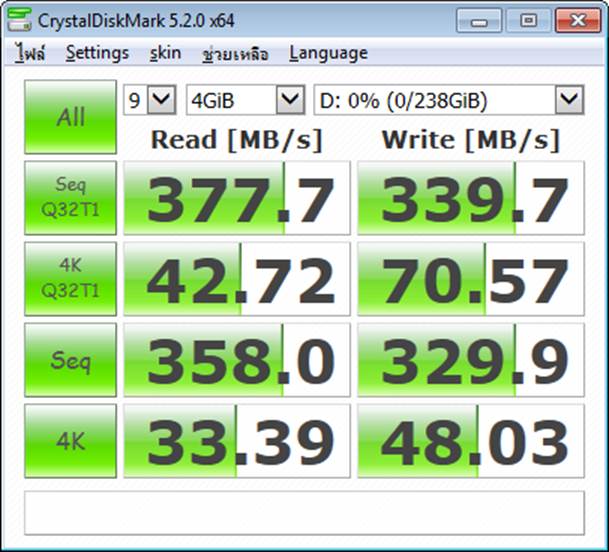
Figure 7 Operation result sample screen
5. Revision History
|
Revision |
Date |
Description |
|
1.0 |
9-May-14 |
Initial release |
|
1.1 |
18-Mar-22 |
Update control Interface form LMB to AXI4-Lite |
Copyright: 2014 Design Gateway Co,Ltd.