SATA-IP Device reference design on AC701 manual
Rev1.0 23-Aug-23
1. Introduction
Serial ATA (SATA) is an evolutionary replacement for the Parallel ATA (PATA) physical storage interface. SATA interface increases speed transfer to be 3.0 Gbps for SATA-II, and 6.0 Gbps for SATA-III. To communication by SATA protocol, there are four layers in its architecture, i.e., Application, Transport, Link, and Phy.
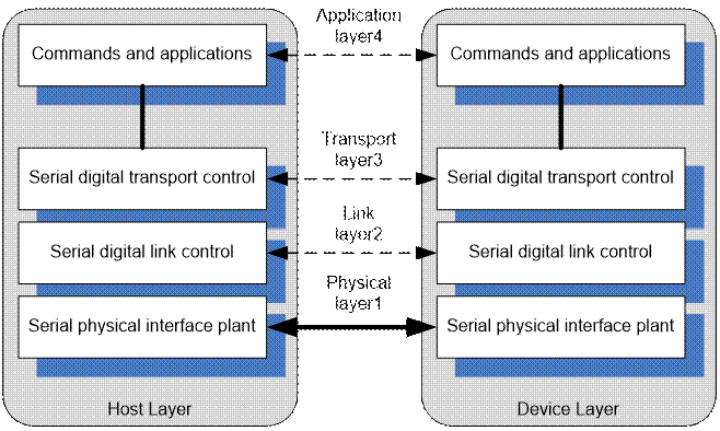
Figure 1‑1 SATA Communication Layer
The Application layer is responsible for overall ATA command execution, including controlling Command Block Register accessed. The Transport layer is responsible for placing control information and data to be transferred between the host and device in a packet/frame, known as a Frame Information Structure (FIS). The Link layer is responsible for taking data from the constructed frames, encoding or decoding each byte using 8b/10b, and inserting control characters such that the 10-bit stream of data may be decoded correctly. The Physical layer is responsible for transmitting and receiving the encoded information as a serial data stream on the wire.
This reference design provides evaluation system which implements all SATA communication layers for Device side to transfer high speed data with SATA-II Host (PC). The SATA-IP core is designed to operate with GTP transceiver of the Artix-7 platform in the reference design on AC701 Evaluation board. More details are described as follows.
2. Environment
This reference design is based on the following environment as shown in Figure2.
l AC701 Platform
l Vivado2019.1
l AB14-CLKSMA board to be clock source for SATA interface
l SATA connector on AB10-PATAFMC, provided by Design Gateway
l SATA standard cable with AB02-CROSSOVER, provided by Design Gateway
l SATA-II Host PC
l micro USB cable for FPGA configuration
l mini USB cable for Serial communication. Set baud rate=115,200 / data=8bit / Non-Parity / Stop=1bit.
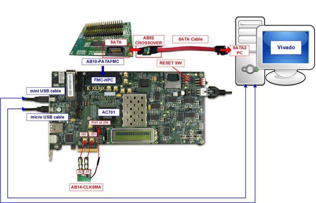
Figure 2‑1 Reference design environment
The procedure for running the demo is described in �SATA-IP Device Demo Instruction on AC701� document.
3. Hardware description
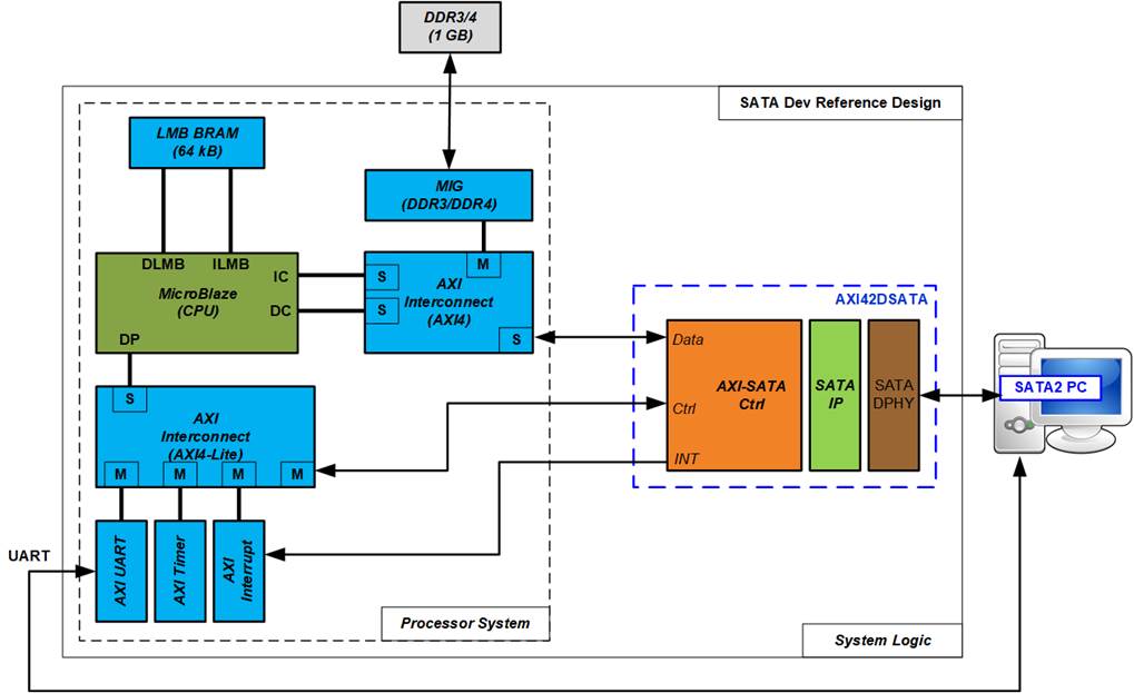
Figure 3‑1 Block diagram of the reference design
l SATA IP device design implementation on Artix-7 FPGA
As shown in Figure 3‑1, the demo system consists of two parts. First is Processor system which consists of the processor and its peripherals. Second is AXI42DSATA module which is hardware logic for interface with SATA-IP.
Processor system has the standard peripherals such as UART, Timer, Interrupt controller, DDR controller, and Block RAM for storing instruction/data of the processor. AXI4-Lite and AXI4 interface in Processor system are exported to connect the hardware logic on top level for control interface and data interface respectively.
AXI4-Lite bus is the simple interface for memory access by single access. Therefore, it is applied to connect to slow-speed CPU peripherals. The control and status registers of AXI42DSATA are connected to the processor by using this bus. While AXI4 bus is more complicate interface that transfers the data as burst mode for high-speed CPU peripherals such as DDR memory. AXI42DSATA transfers the data with DDR memory by using AXI4 bus in master mode to achieve high-speed performance. Therefore, AXI4-Lite and AXI4 interface are exported from processor system to connect to AXI42DSATA in HDL code of System logic which is the top module. The details of SATA-IP device demo are described as follows.
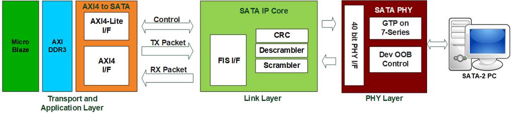
Figure 3‑2 SATA-IP interface for SATA device demo
l PHY Layer
This layer is designed by using GTP module (built-in high speed serial circuit) of Artix-7 device, operating with logic control to generate OOB (out-of-band) sequence and initialization sequence of physical layer. State machine to control the OOB sequence is designed in �dev_oob_control.vhd�. The device OOB sequence is designed in the opposite side of the host OOB sequence. Besides, �gtp_rxreset_seq.vhd� is designed to control reset sequence at Rx interface of GTP module. The top module of PHY layer is �sata2dphy_A7.vhd� which includes OOB module, reset sequence module, and GTP module for running SATA device PHY operation at SATA-II speed.
The reference design follows PLL and GTP reset sequence described in �7 Series FPGAs GTP Transceivers� user guide, refer to �Reset and Initialization� section in ug482 for detailed reset sequence.
Before building user board, user must read carefully and must follow design guide line described in UG482 (7 Series FPGAs GTP Transceivers User Guide).
l Link Layer by SATA-IP
Link Layer and a part of Transport layer are implemented by SATA-IP. To send FIS packet, the user packet is converted to PHY layer packet format by including CRC and scrambling the data. On the contrary, packet from PHY layer is decoded and re-arrange to FIS packet format for SATA user interface. More details about SATA-IP are described in �dg_sata_ip_data_sheet_7series_en� document.
l Transport Layer by AXI42DSATA
AXI42DSATA is the logic design to connect SATA-IP interface to standard interface within CPU system, i.e., AXI4-Lite interface for control/status signals with the processor and AXI4 interface (master mode) for data signals with DDR controller.
Table 3‑1 Register mapping from CPU side
|
Address |
Register Name |
Description (Bit order is little endian) |
|
Rd/Wr |
(Label in the �sata_device.c� ) |
|
|
BA+0x04 |
Error Code Reg. |
SATA IP Error code after finishing packet transmission/reception to detect CRC or FIS error. |
|
Rd |
(ERROR_CODE) |
|
|
BA+0x0C |
Receive Word Count Reg. |
[31] : Received FIS type in the interrupt (�1�: Non-Data FIS, �0�: Data FIS). This bit is cleared by asserting bit[29] of INT_CLEAR to �1�. [23:0] : Total received word count of FIS data. Auto clear after starting then next transfer (CONTROL Reg is written). |
|
Rd |
(RX_COUNT) |
|
|
BA+0x00 |
Transmit Data Address Reg. |
Set DDR start address of transmit FIS data area Bit[8:0] of this value needs to be equal to 0. |
|
Wr |
(TX_ADDR) |
|
|
BA+0x04 |
Received Data Address1 Reg. |
Set DDR start address of received other FIS area (except DATA FIS type). Bit[8:0] of this value needs to be equal to 0. |
|
Wr |
(RX_ADDR) |
|
|
BA+0x08 |
Control Reg. |
[31] : Hardware Reset [30] : Start Transmit data [29] : FIS type (�1�: Data, �0�: Others) [15:0] : Total Transmit word count. RX_COUNT register is cleared by write operation to this register |
|
Wr |
(CONTROL) |
|
|
BA+0x0C |
Received Data Address2 Reg. |
Set DDR start address of received DATA FIS area Bit[8:0] of this value needs to be equal to 0. |
|
Wr |
(RX2_ADDR) |
|
|
BA+0x10 |
Interrupt Clear Reg |
[31] : Set this bit to clear ip2host interrupt [30] : Set this bit to clear host2ip interrupt [29] : Set this bit to clear received FIS type |
|
Wr |
(INT_CLEAR) |
(BA : Base Address)
Register map of control signals to interface with MicroBlaze is shown in Table 3‑1. Main operation of these registers is to define DDR address for transferring FIS data, transfer length, and FIS type (data or non-data). Besides, the registers are read by MicroBlaze to check the status signals of AXI42DSATA. The non-data FIS is stored in reserved area of DDR while the data FIS is stored in RAMDISK area of DDR, as shown in Figure 3‑3.
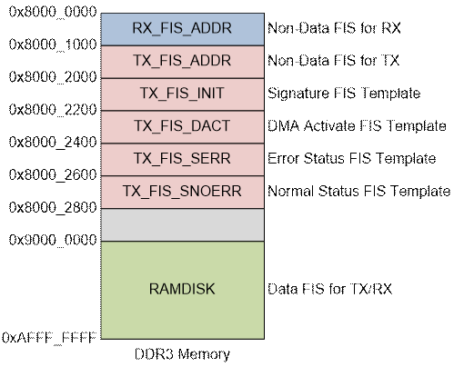
Figure 3‑3 DDR Memory Map in SATA device demo
The reserved area to store non-data FIS for both TX and RX direction is defined to the first 256 MB of DDR. The remaining 768 MB of DDR is defined to be RAMDISK area. To improve performance, the frequently used TX FIS such as Status FIS and DMA Activate FIS are pre-created and stored in specific DDR address without modification. Therefore, MicroBlaze does not need to re-create this FIS for transmitting to SATA Host.
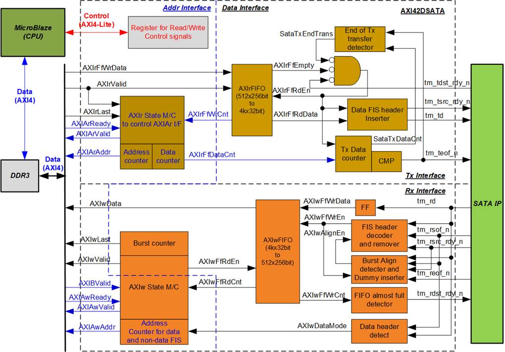
Figure 3‑4 Block diagram of AXI42DSATA
To transfer data by AXI4 interface in master mode, all signals are divided into four groups, i.e., AXIAr (Read address interface), AXIr (Read data interface), AXIAw (Write address interface), and and AXIw (Write data interface). The address request of write and read interface is controlled by state machine. While data interface uses two FIFOs for buffering the data transmission between DDR and SATA-IP. The FIFOs are asymmetric which has different bus size for write and read interface because data width of AXI4 bus is 256 bits while data width of SATA-IP is 32 bits.
To receive data from DDR to SATA-IP, MicroBlaze sets control register to start transferring data operation. State Machine sends data request to get data from DDR to store to AXIrFIFO. The data request is created until total number of requested data is equal to the set value from user. Before creating the new request, FIFO status is monitored. The request will be paused if FIFO is almost full. Read enable signal of AXIrFIFO is simple designed by monitoring Empty flag of FIFO with data ready signal from SATA-IP. Therefore, data is always transferred if the FIFO has the data and SATA-IP is ready. The data output from AXIrFIFO is appended by Data FIS header to create complete data FIS packet by the logic when user setting is sending Data FIS type. Also, End-of-packet signal is asserted to SATA-IP when the data counter shows the last data is transmitted. Therefore, MicroBlaze can simply create any FIS type with specified FIS size to SATA host through SATA-IP.
When data is transferred from SATA Host to DDR, the FIS header of a received packet is decoded by the logic to check FIS type. AXIwDataMode, output signal from the decoder, is fed to address generator for selecting the destination DDR address for storing the packet. Data FIS packet is stored at RAMDISK area while non-Data FIS packet is stored at RX_FIS_ADDR area. Before storing the packet to RAMDISK area and AXIwFIFO, the Data FIS header is removed from FIS packet. In this demo, the burst size for transferring data with DDR is fixed to 16x256-bit beat. Therefore, when the receive packet size is not aligned to burst size, the logic will add dummy word to AXIwFIFO for data alignment. Similar to AXIr interface, the state machine is applied to control AXIw interface. It monitors read counter of AXIwFIFO until the data is enough for one burst size. After that, it sends request to DDR to start data transferring from AXIwFIFO to DDR. After finishing one burst size transferring, the state machine goes to Idle state. MicroBlaze decodes the received FIS packet when interrupt is asserted and total number of received size is applied to check that all received packet are processed completely.
AXI42DSATA logic including SATA-IP and PHY layer are designed in HDL code of �AXI2SATA.vhd�, provided to user as delivery item.
4. Software description
l SATA Device operation
Basically, SATA Device must support all mandatory commands sent from the Host. However, this reference design supports the minimum command to simplify the MicroBlaze firmware. Therefore, user can easily understand fundamental SATA Device software operation.
Similar to SATA Host reference design, the communication between the Host and the Device via SATA is done by FIS (Frame Information Structure) data structure. MicroBlaze in the Device design builds FIS data structure on its main memory space (DDR), and then sends it to the Host by DMA controller that operates in master mode. On the contrary, FIS data sent from the SATA Host is also transferred to the main memory (DDR) by DMA controller.
MicroBlaze in the SATA Device operates in following steps.
(1) After boot-up, send RegD2H FIS to the Host.
(2) Wait command receive.
(3) Execute received command operation.
(4) Send FIS Data
(5) Additional FIS data transmit/receive if necessary.
l Software of reference design description
Software source code of this reference design is stored in �sata_device.c�. As a minimum implementation, this source code has a following limitation.
- There is no optional function support such as S.M.A.R.T (Self-monitoring, Analysis and Reporting Technology)
- 48bit LBA is not supported
- Cache is not supported (Not need because this peripheral is RAMDISK)
- Ultra DMA mode support is Mode 5 or slower.
After Link is established, software sends RegD2H (Device to Host FIS), and then processes command sent from the Host. This design prepares original IDENTIFY DEVICE data to limit operation from the Host. Since DDR memory capacity on FPGA is 1GBytes and some area is applied to store FIS packet with SATA-IP, this software declares only 768MBytes for disk capacity.
To make easy implementation, maximum value of SET MULTIPLE MODE is set to 1 so that READ/WRITE SECTOR command sequence and READ/WRITE MULTIPLE command sequence is identical. In this case, performance is not good. However, in practically there is no problem for typical use because the Host uses UDMA mode rather than legacy PIO mode.
There are two READ/WRITE address modes, i.e., CHS (Cylinder/Head/Sector) mode and LBA (Logical Block Address) mode. Generally, CHS mode is used in the small size HDD access. For this reference design, CHS is converted to be LBA mode access.
The commands implemented in this reference design are READ SECTOR, READ MULTIPLE, WRITE SECTOR, WRITE MULTIPLE, READ DMA, and WRITE DMA. For the other mandatory commands, this reference design has no operation and simply returns RegD2H without error. For other commands which are not mandatory command, this reference design returns RegD2H with error.
This reference design implements the minimum command for simple board operation check. User should modify to support all the mandatory commands defined in the ATA Standard specification in the application.
5. Real board operation
l OS Boot-up
After Windows10 boot-up completion, user can recognize that Windows10 can detect FPGA board as a SATA Device and transfer mode is set to Ultra DMA Mode 5, as shown in Figure 5‑1. Some mandatory commands for OS Boot-up are shown in Table 5‑1. The command sequence depends on PC, Device, and OS.
Table 5‑1 Command Sample for Windows10 Boot-up
|
Command code |
Command operation |
|
ECh |
IDENTIFY DEVICE |
|
EFh |
SET FEATURES (Set transfer mode) |
|
F5h |
SECURITY FREEZE LOCK |
|
C8h |
READ DMA |
Transfer mode settings is sent after IDENTIFY DEVICE command. Though this reference design does not support optional S.M.A.R.T command, OS boot-up is successful. This reference design sends error response of command that does not support by RegD2H. This design simply returns RegD2H without error when receiving SECURITY FREEZE LOCK command.
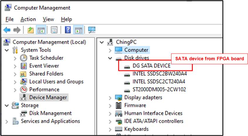
Figure 5‑1 Windows10 detects FPGA board as SATA Device
After Windows10 boot-up completion, user can recognize that Windows10 detects FPGA as a SATA Device and transfer mode is set to Ultra DMA Mode 5.
l OS Format operation
Table 5‑2 shows a command sample for Format operation. Test results are shown in Figure 5‑2.
Table 5‑2 Command Sample for Format
|
Command code |
Command operation |
|
C8h |
READ DMA |
|
CAh |
WRITE DMA |
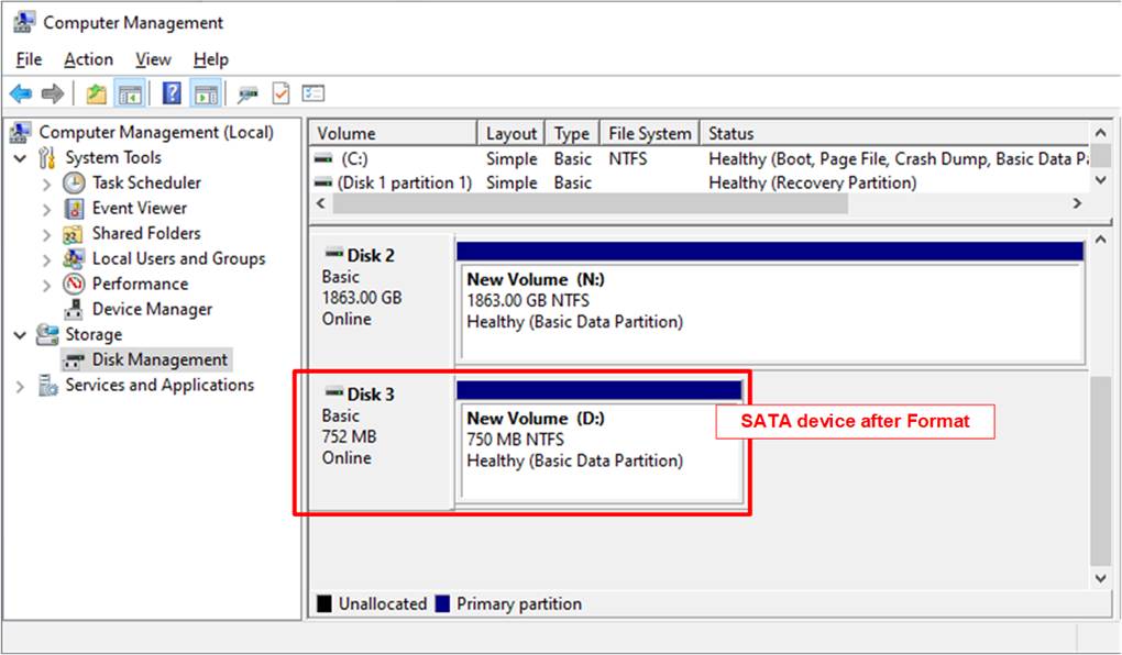
Figure 5‑2 New drive is displayed after Format
l OS Shutdown operation
Table 5‑3 shows command sample when Windows10 shut down. Windows10 executes remained write data, and then execute STANDBY IMMEDIATE command.
Table 5‑3 Command Sample when Windows10 shut down
|
Command code |
Command operation |
|
CAh |
WRITE DMA |
|
E0h |
STANDBY IMMEDIATE |
l Performance result
Figure 5‑3 shows test result performance of this reference design on AC701 (SATA-II speed).
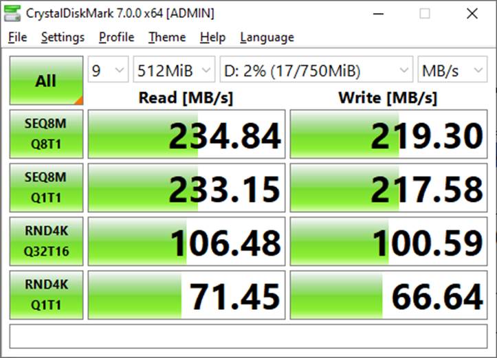
Figure 5‑3 Performance result of read/write data transfer
6. Revision History
|
Revision |
Date |
Description |
|
1.0 |
17-Jun-21 |
Initial release |