HCTL-IP RAID0x8 DDR reference design manual
Rev1.0 22-Aug-23
1 Introduction
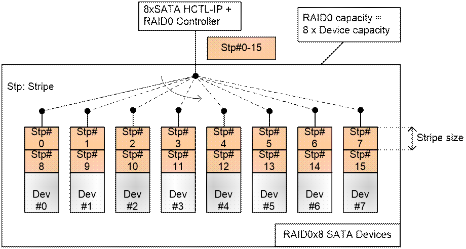
Figure 1‑1 RAID0 by 8 SATA devices data format
RAID0 system uses multiple storages to extend total storage capacity and to increase write/read performance. Assumed that total number of device is N, total storage capacity is equal to N multiply by amount of storage. Write and read speed are almost equal to N multiply by speed of one device.
Data format of RAID0 is shown in Figure 1‑1. Data stream of the host side are split into a small stripe and transfer to one device at a time. Stripe size is the data size to store in one device before switching to other devices.
In the reference design, eight devices are applied to run RAID0 system. Stripe size is equal to 512 byte (one sector). All devices connecting in the system should be same model to match characteristic and get the best performance and capacity. By using RAID0 reference design, the total capacity is equal to eight times of one device capacity and the performance result for write and read are almost eight times of one device performance.
This demo includes DDR to be the buffer of the system to support ultra speed transferring with sustain rate. DDR is used to be the buffer when the device is not ready to access especially during flush operation from internal cache in Write command. The system is suitable for the application which requires sustain rate such as data logger from high-speed A/D.
Before running the reference design, it is recommended to study SATA HCTL-IP datasheet and single channel demo firstly from following link.
http://www.dgway.com/products/IP/SATA-IP/dg_sata_host_ip_data_sheet_en.pdf
http://www.dgway.com/products/IP/SATA-IP/dg_satahostip_refdesign_en.pdf
http://www.dgway.com/products/IP/SATA-IP/dg_satahostip_instruction_en.pdf
2 Hardware overview
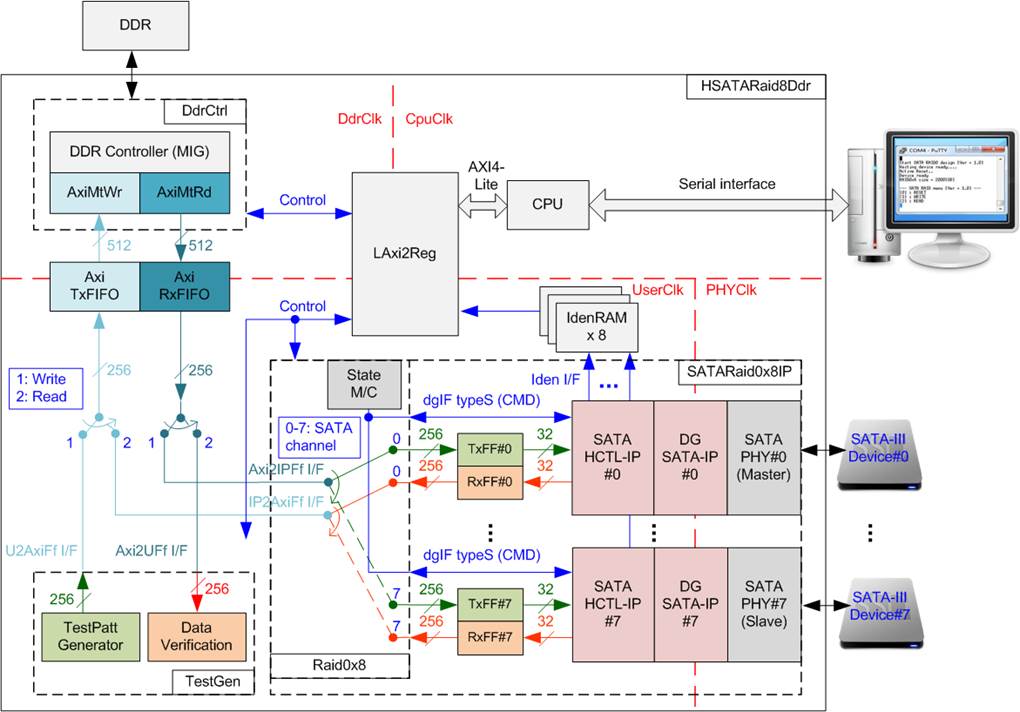
Figure 2‑1 HCTL-IP RAID0x8 with DDR demo hardware
The hardware system can be split into four groups following the interface i.e.
1) TestGen: The example of user logic to write and read data in this reference design is TestGen module. TestGen module generates test data at sustain rate to DDR in Write command. For Read command, TestGen also reads and verifies test data from DDR at sustain rate. TestGen uses 256-bit data bus and runs in UserClk domain which is equal to 200 MHz.
2) RAID: Eight SATA HCTL-IPs are applied to control eight SATA-III devices. Raid0x8 arranges data stored in eight devices as RAID0 format. Raid0x8 decodes the current address to select one SATA device to transfer data with DDR. Data bus size of RAID0 is 256-bit which is eight times of SATA HCTL-IP to match data bandwidth with eight SATA devices. Two FIFOs (TxFF and RxFF) are connected between Raid0x8 and SATA HCTL-IP to convert data bus size.
3) DdrCtrl: DDR controller in reference design uses 512-bit AXI4 bus to be user interface. AxiMtWr is designed to transfer data from AxiTxFIFO to DDR while AxiMtRd is designed to transfer data from DDR to AxiRxFIFO. The source of AxiTxFIFO and the destination of AxiRxFIFO are switched between TestGen and RAID block following the command. For Write command, Data from TestGen is stored to DDR through AxiTxFIFO and Read data from DDR is forwarded to RAID block through AxiRxFIFO. For Read command, DDR is written by RAID block and read by TestGen.
4) CPU: Test operation in the demo is controlled by user through Serial console. CPU firmware is designed to receive test parameters and the command from user. CPU sets parameters to the hardware through AXI4-Lite bus. LAxi2Reg has the register sets of test parameters which are mapped to different address of CPU. LAxi2Reg decodes the address of AXI4-Lite bus to select the active parameter. For write access, Write data from AXI4-Lite bus is set to the selected parameter following the address. For read access, Read data from selected parameter is returned to AXI4-Lite bus. Read access is applied for CPU monitoring and displaying the hardware status to the user through Serial console.
More details of the hardware are described as follows.
2.1 TestGen
This module is designed to generate Test pattern to WrFf as constant rate in Write command. For Read command, this module reads data from RdFf as constant rate and verifies the data with Test pattern. The details of hardware inside TestGen are shown in Figure 2‑2.
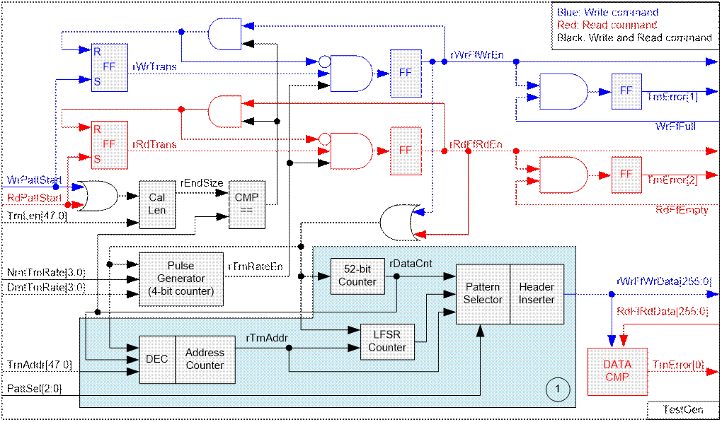
Figure 2‑2 TestGen hardware
Pulse Generator (bottom left block) is designed to generate enable pulse (rTrnRateEn) to control data rate for writing and reading FIFO. As shown in Figure 2‑3, duty cycle of rTrnRateEn is controlled by NmtTrnRate and DmtTrnRate value, set by user. rTrnRateEn is used to be enable signal to assert rWrFfWrEn and rRdFfRdEn to ‘1’. So, maximum data rate of rWrFfWrEn and rRdFfRdEn is equal to (NmtTrnRate/DmtTrnRate) x Clock Frequency (200 MHz) x 256-bit.
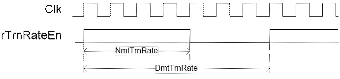
Figure 2‑3 rTrnRateEn Timing diagram
The logic to generate rWrFfWrEn and rRdFfRdEn is shown in upper side in blue and red color sequentially. For Write command, WrPattStart is asserted to ‘1’ as a pulse. rWrTrans is asserted to ‘1’ by WrPattStart to start writing FIFO signal. rWrTrans is de-asserted to ‘0’ when last data is written to FIFO, monitored by comparing rDataCnt (counter to check current data size) with rEndSize (total data size setting from user). Timing diagram of rWrTrans is shown in Figure 2‑4.
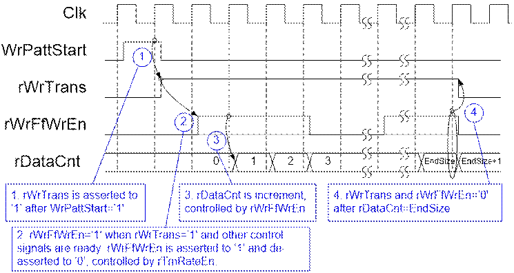
Figure 2‑4 rWrTrans Timing diagram
rWrFfWrEn is controlled by rWrTrans and rTrnRateEn. When rWrTrans=’1’, rWrFfWrEn timing is same as rTrnRateEn to write data to FIFO as constant rate. rDataCnt is up-counter, controlled by rWrFfWrEn during Write command. After last data is transferred, rWrFfWrEn and rWrTrans are de-asserted to ‘0’ to finish write operation.
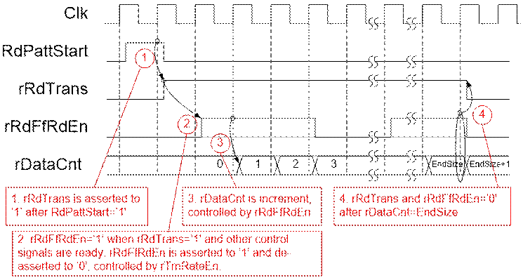
Figure 2‑5 rRdTrans Timing diagram
Similar to rWrTrans, rRdTrans timing diagram is shown in Figure 2‑5. rRdTrans is asserted to allow the logic to read data from FIFO as constant rate. rRdFfRdEn is asserted to ‘1’ when rRdTrans=’1’ and rTrnRateEn=’1’. rDataCnt is the counter to check total data. rRdFfRdEn and rRdTrans are de-asserted to ‘0’ after last data is received.
As shown in upper right side of Figure 2‑2, TrnError[1] is asserted when WrFfFull is equal to ‘1’ during writing in sustain rate to show that system cannot operate Write command in this rate correctly. Also, TrnError[2] is asserted when RdFfEmpty is equal to ‘1’ during reading in sustain rate to show that system cannot operate Read command in this rate correctly.
Block no.1 in lower side of Figure 2‑2 shows the logic for generating test pattern in TestGen module. To create unique test data for each sector, test pattern in this demo is designed as shown in Figure 2‑6.
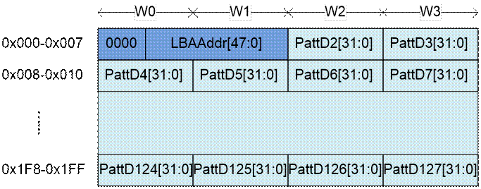
Figure 2‑6 Test pattern format in each sector
Test pattern consists of two parts, i.e. 64-bit header in word#0 and word#1 of each sector and test data in word#2 – word#127. 64-bit header is created by using LBA address value of the data (LBA address is the address in sector unit). As shown in Figure 2‑2, rTrnAddr is loaded to TestGen module to create 64-bit header value for the 1st sector data. rTrnAddr is increased after completing to transferring one sector data. So, the logic to create rTrnAddr needs to monitor rDataCnt and write/read enable signal to know the end of one sector transfer.
TestGen supports to generate five patterns, i.e. 32-bit increment, 32-bit decrement, all 0, all 1, and 32-bit LFSR. 32-bit increment is generated by using lower-bit of rTrnAddr and rDataCnt. Decrement pattern is designed by using NOT logic with increment data. To create 32-bit LFSR counter, 256-bit data is designed by using two sets of 32-bit LFSR pattern as shown in Figure 2‑7.
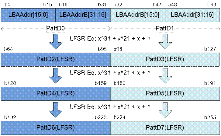
Figure 2‑7 LFSR pattern in TestGen
Start value of LFSR is designed by using combination signal of 32-bit LBA address and NOT logic of LBA address (LBAAddrB means NOT logic of LBAAddr signal). PattD0/D2/D4/D6 are the sequence of LFSR counter set#0 which using LBAAddr[15:0] and NOT LBAAddr[31:16] to be start value. PattD1/D3/D5/D7 are the sequence of LFSR counter set#1 which using NOT LBAAddr[15:0] and LBAAddr[31:16] to be start value. 256-bit data is generated within one clock, so PattD2-D7 must design the logic to calculate 32-bit LFSR pattern as look-ahead style.
3-bit PattSel signal are used to select one of five test patterns. Header Inserter logic inserts 64-bit header to be the 1st data of each sector. After that, test data from pattern counter is transferred to rWrFfWrData. In Read command, rWrFfWrData is used to be expected value to compare with read data from FIFO (RdFfRdData). TrnError[0] is asserted to ‘1’ when data verification is failed.
2.2 RAID
User interface of RAID is designed by using dgIF typeS format. CMD interface is connected to LAxi2Reg to receive the parameter from user through Serial console. Data bus size of RAID block is 256-bit which is connected with AxiRxFIFO and AxiTxFIFO. Another side of RAID is connected to eight SATA devices. The system includes eight IdenRAMs for receiving Iden I/F of SATA HCTL#0 - #7. The hardware details of RAID are shown in Figure 2‑8.
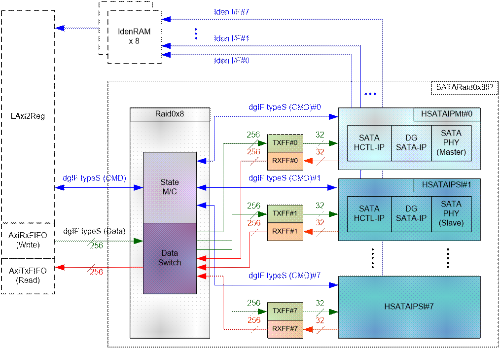
Figure 2‑8 RAID hardware
The hardware inside RAID consists of three modules, i.e. Raid0x8, eight sets of FIFO, and eight sets of HSATAIP.
2.2.1 HSATAIP
HSATAIP is the group of complete HDL for SATA application. It consists of SATA HCTL-IP, SATA-IP, and SATAPHY. More details of SATA HCTL-IP are described in datasheet.
http://www.dgway.com/products/IP/SATA-IP/dg_sata_host_ip_data_sheet_en.pdf
HSATAIP has two HDL codes because of different SATA PHY. There are two types of SATA PHY in RAID design, i.e. Master and Slave. All SATA PHYs use same clock source for transceiver operation. Clock source is created in Master PHY and then forwarded to all Slave PHYs.
2.2.2 FIFO
Two FIFOs are applied for one SATA channel. TxFIFO is designed to convert 256-bit data which is Raid0x8 bus size to 32-bit data which is HSATAIP bus size. FIFO size is 16 kByte, so it can store data up to 31 sectors. RxFIFO size is same as TxFIFO, but it converts data from 32-bit to 256-bit.
2.2.3 Raid0x8
Raid0x8 consists of state machine for controlling command interface and Data Switch to controlling data interface.
After receiving new command request from LAxi2Reg, state machine decodes the parameters and then calculates the address and transfer length of each HSATAIP. After that, state machine generates command request with the valid address and length to all HSATAIPs.
Next, state machine is responsible to control Data Switch for selecting the active SATA channel. State machine needs to calculate the current sector address by loading the start value from LAxi2Reg and then increased after completing to transfer one sector data with AxiTxFIFO/AxiRxFIFO. Three lower bit of current sector are used to select SATA channel, i.e. “000” for HSATAIP#0, “001” for HSATAIP#1, …, “111” for HSATAIP#7.
There are many pipeline registers to switch data bus of each SATA channel. The overhead time from pipeline register and control signal is about 6 clock cycles for transferring 512-byte data (16x256-bit). To compensate this overhead time, clock domain to run Raid0x8 must be more than 150 MHz which is SATA PHY clock. It is recommended to set clock frequency more than 190 MHz to compensate 27% overhead time (6 / (16+6) = 27%). In the reference design, Raid0x8 clock frequency is set to 200 MHz.
The user interface of Raid0x8 is shown in Table 2‑1. Command and data interface are designed as dgIF typeS format. The status and Iden port of all SATA HCTL-IP are mapped to user interface directly to monitor each SATA device status independently.
Table 2‑1 Signal description of Raid0x8 (only user interface)
|
Signal |
Dir |
Description |
|
User Interface |
||
|
RstB |
In |
Reset signal. Active low. Please use same reset signal as SATA HCTL-IP. |
|
Clk |
In |
User clock. Must use the same clock as SATA HCTL-IP. |
|
dgIF typeS |
||
|
UserCmd[1:0] |
In |
User Command. “00”: Identify device command, “01”: Security erase “10”: Write device, “11”: Read device. |
|
UserAddr[47:0] |
In |
Start address of device to write/read in sector unit (512 byte). |
|
UserLen[47:0] |
In |
Total transfer size in the request in sector unit (512 byte). Valid from 1 to (LBASize-UserAddr). |
|
UserReq |
In |
Request the new command. Can be asserted only when the IP is Idle (UserBusy=’0’). Asserted with valid value on UserCmd/UserAddr/UserLen signals. |
|
UserBusy |
Out |
IP Busy status. New request will not be allowed if this signal is asserted to ‘1’. |
|
LBASize[47:0] |
Out |
Total device capacity in sector unit (512 byte). Default value is 0. This value is equal to eight times of LBASize value output from IP#0. |
|
UserError |
Out |
Error flag. Assert when UserErrorType is not equal to 0. The flag can be reset only by de-asserting RstB to ‘0’. |
|
UserErrorType[63:0] |
Out |
Error status which are mapped from status in each SATA HCTL-IP. One byte is mapped to UserErrorType[7:0] from one IP. IP#0 is mapped to the lowest bye while IP#7 is mapped to the highest byte. [7:0] – Mapped from UserErrorType[7:0] of IP#0. [15:8] – Mapped from UserErrorType[7:0] of IP#1. … [63:56] – Mapped from UserErrorType[7:0] of IP#7. |
|
UserFifoWrCnt[15:0] |
In |
Write data counter of User received FIFO. Used to check FIFO space size. If total size is less than 16-bit, please fill ‘1’ to upper bit. UserFifoWrEn can be asserted when UserFifoWrCnt[15:5] is not equal to all 1. |
|
UserFifoWrEn |
Out |
Write data valid of User received FIFO |
|
UserFifoWrData[255:0] |
Out |
Write data bus of User received FIFO. Synchronous to UserFifoWrEn. |
|
UserFifoRdCnt[15:0] |
In |
Read data counter of User transmit FIFO. Used to check data available size in FIFO. If total FIFO size is less than 16-bit, please fill ‘0’ to upper bit. UserFifoRdEn can be asserted when UserFifoRdCnt[15:4] is not equal to 0. |
|
UserFifoEmpty |
In |
FIFO empty flag of User transmit FIFO. This signal is unused in the design. |
|
UserFifoRdEn |
Out |
Read valid of User transmit FIFO |
|
UserFifoRdData[255:0] |
In |
Read data returned from User transmit FIFO. Valid after UserFifoRdEn asserted one clock cycle. |
|
Other Interface |
||
|
TestPin[0-7][31:0] |
Out |
Direct mapped from TestPin in each SATA HCTL-IP. Index 0-7 is referred to IP number. [0]-IP#0, [1]-IP#1, … , [7]-IP#7. |
|
TimeOutSet[31:0] |
Out |
Timeout value of all SATA HCTL-IPs. Time unit is following Clk frequency value. |
|
TrnLinkup[7:0] |
Out |
Linkup signal from trn_link_up in each SATA-IP. Index 0-7 is referred to IP number. [0]-IP#0, [1]-IP#1, … , [7]-IP#7. |
|
IdenWrAddr[0-7][6:0] |
Out |
Direct mapped from IdenWrAddr in each SATA HCTL-IP. Index 0-7 is referred to IP number. [0]-IP#0, [1]-IP#1, … , [7]-IP#7. |
|
IdenWrEn[7:0] |
Out |
Direct mapped from IdenWrEn in each SATA HCTL-IP. Index 0-7 is referred to IP number. [0]-IP#0, [1]-IP#1, … , [7]-IP#7. |
|
IdenWrData[0-7][31:0] |
Out |
Direct mapped from IdenWrData in each SATA HCTL-IP. Index 0-7 is referred to IP number. [0]-IP#0, [1]-IP#1, … , [7]-IP#7. |
Timing diagram of user interface and Identify device interface are similar to SATA HCTL-IP.
Please see more details from SATA HCTL-IP datasheet. Data interface for RAID operation are shown as follows.
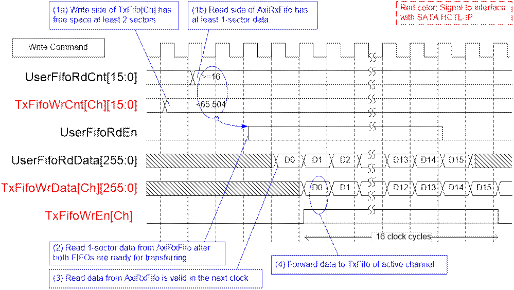
Figure 2‑9 Raid0x8 data timing diagram of Write command
When user sends Write command to RAID, data is forwarded from AxiRxFIFO to TxFifo[0]-[7]. One TxFifo is active to transfer one sector data and the active SATA channel is switched to next channel for transferring next sector following RAID0 behavior. Before forwarding data, UserFifoRdCnt and TxFifoWrCnt of active channel are monitored to confirm that at least 1 sector data is stored in AxiRxFIFO and at least 2-sector free space is available in TxFifo of active channel. UserFifoRdEn is asserted for 16 clock cycles to transfer 512-byte data continuously.
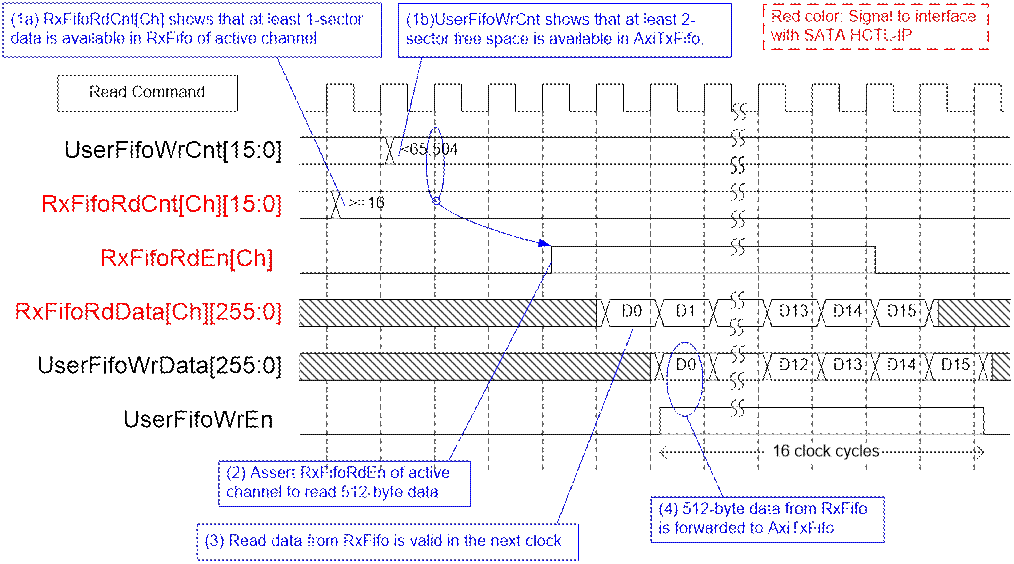
Figure 2‑10 Raid0x8 data timing diagram of Read command
When user sends Read command to RAID, data is forwarded from RxFifo[0]-[7] to AxiTxFifo, as shown in Figure 2‑10. Similar to Write command, one RxFifo is active for each 512-byte transfer, and then active SATA channel is switched to the next channel for next sector transfer. Before forwarding data, UserFifoWrCnt and RxFifoRdCnt of active channel are monitored to confirm that at least 1 sector data is available in RxFifo of active channel and at least 2-sector free space is available in AxiTxFifo. UserFifoWrEn is asserted for 16 clock cycles to transfer 512-byte data continuously.
2.3 DdrCtrl
This module is designed to interface with DDR memory which is the data buffer to support transferring data as sustain rate in this system. MIG is Xilinx IPcore to control external memory such as DDR4. The IP includes clock generator to generate many clocks for interfacing with DDR. So, this reference design uses clock generator inside MIG to create clock domain for using in the system, i.e. UserClk which is 200 MHz for user logic and CpuClk which is 100 MHz for CPU system. AxiClk is auto generated by MIG to be clock source for interfacing with MIG. AxiClk frequency is 300 MHz for running DDR4 at 1200 MHz.
AxiMtWr and AxiMtRd are designed to decode the command request from LAxi2Reg and transfer data with MIG through AXI4 interface. AxiMtWr is connected to Write port of AXI4 bus for transferring data from AxiTxFIFO to MIG. AxiMtRd is connected to Read port of AXI4 bus for transferring data from MIG to AxiRxFIFO. AxiMtWr and AxiMtRd run in AxiClk domain which is very high frequency, so the logic includes many pipeline registers.
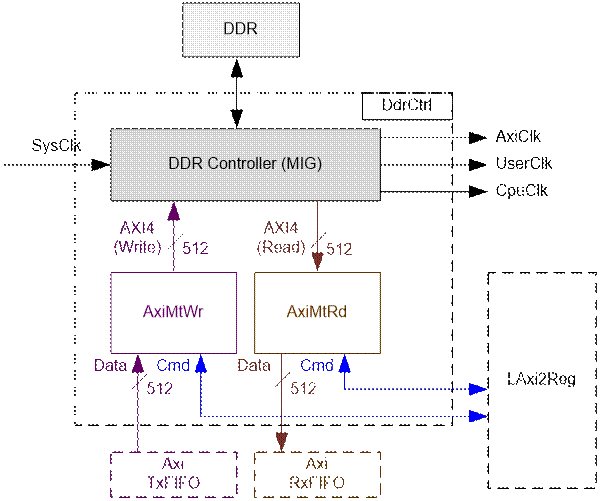
Figure 2‑11 DdrCtrl hardware
2.3.1 AxiMtWr
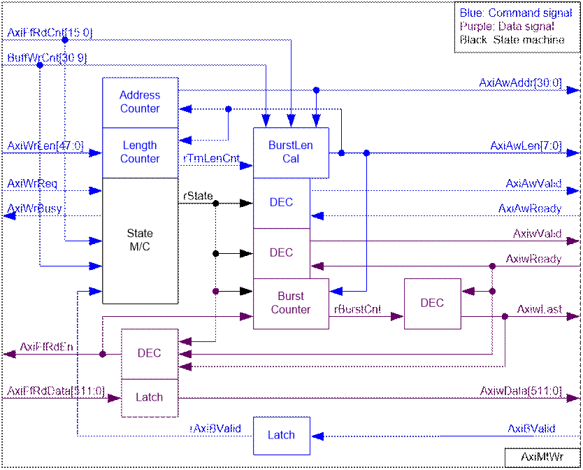
Figure 2‑12 AxiMtWr hardware
As shown in Figure 2‑12, state machine is designed in AxiMtWr to control the sequence for write transferring through AXI4 bus interface. The signal of AXI4 can be separated into two groups, i.e. command and data signals. Command signal is in blue color at upper side and data signal is in purple color at lower side.
The sequence to transfer AXI4 interface is sending address and control (AxiAwAddr, AxiAwLen, AxiAwValid), sending data (AxiwData, AxiwValid), and waiting response (AxiBValid). State machine is designed following AXI4 interface sequence. After new write request (AxiWrReq) is detected, state machine changes to transfer state. At the same time, Length counter loads set value of total transfer size (AxiWrLen) and Address counter are reset to 0 to prepare the new transfer. Before transferring one burst size data, state machine checks that data in AxiTxFIFO is enough by monitoring AxiFfRdCnt and DDR is not full by monitoring BuffWrCnt. Then, state machine generates write request to DDR (AxiAwValid) with the valid value of DDR address (AxiAwAddr) and length (AxiAwLen).
Data from AxiTxFIFO is transferred to DDR by asserting AxiwFfRdEn=’1’ to read data from FIFO and then asserting AxiwValid=’1’ to transfer data to DDR. Data from AxiTxFIFO is latched to Flip-Flop before forwarding to DDR (AxiwData) to solve timing constraint problem. AxiMtWr runs in DdrClk which is high frequency (300 MHz). rBurstCnt is designed to count the data in one burst transfer for asserting AxiwLast=’1’ when transferring the last data in the burst. AxiBValid is asserted to ‘1’ by DDR after receive all data in the request.
From above sequence, address, data, and response are transferred sequentially by using one state machine, not pipelined transfer. To reduce the effect of overhead time from address and response to data performance, the maximum burst size could be extended to 4kByte size. BurstLen Cal block calculates burst size to be 512 byte, 1 kByte, 2 kByte, and 4 kByte depending on FIFO/DDR status, current address alignment, and remaining transfer size. Using bigger burst size reduces the effect of overhead time to transfer performance. Burst size is set to 4 kByte when following conditions are met.
1) Remaining transfer size is more than or equal to 4 kByte (rTrnLenCnt[47:3] is not equal to 0).
2) Current address is aligned to 4 kByte (AxiAwAddr[11:0] is equal to 0).
3) AxiFfRdCnt value is more than or equal to 4 kByte (AxiFfRdCnt[15:6] is not equal to 0).
4) BuffWrCnt value shows that at least 8 kByte free space is found (BuffWrCnt[30:13] is not equal to all 1).
The output of BurstLen Cal is AxiAwLen signal. AxiAwLen is also used to calculate the next address in Address counter and calculate remaining transfer size in Length counter.
The operation of the logic inside AxiMtWr is displayed as timing diagram in Figure 2‑13. In the example, burst size is equal to 8 for transferring 512 byte data.
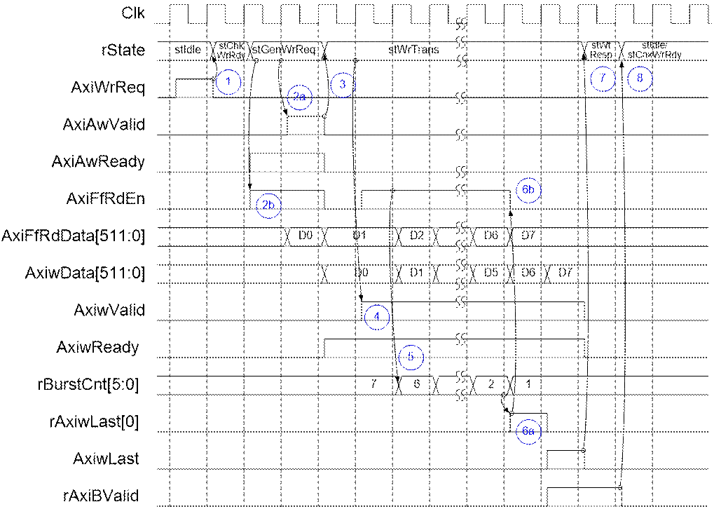
Figure 2‑13 AxiMtWr Timing diagram when burst size = 512 byte
After AxiWrReq is asserted to ‘1’, state machine changes to stChkWrRdy to monitor data size in FIFO and DDR. If FIFO and DDR are ready to transfer one sector data, state machine will change to next state. stGenWrReq is designed for two functions, i.e. asserting AxiAwValid=’1’ for write request until AxiAwReady=’1’ and asserting AxiFfRdEn=1’ for two clock cycles to read two data from AxiTxFIFO. After write request is received (AxiAwValid=’1’ and AxiAwReady=’1’), state machine changes to stWrTrans to transfer 8 data.
AxiwValid is asserted to ‘1’ in stWrTrans with the valid value of AxiwData which stores previous data of AxiFfRdData. During transferring, rBurstCnt is decrement, controlled by AxiFfRdEn signal. When rBurstCnt=2 and AxiwReady=’1’, rAxiwLast[0] is asserted to ‘1’ to pause data reading from FIFO (AxiFfRdEn=’0’). AxiwLast which stores the previous status of rAxiwLast[0] is asserted with the last data available on the bus in the next transfer cycle to complete data transfer.
State machine changes to stWtResp to wait AxiBValid asserting to ‘1’ after completing the last data. State machine changes from stWtResp to stIdle when total data are transferred. If it is not last transaction, state machine will go back to stChkWrRdy to send next request and next data to DDR.
2.3.2 AxiMtRd
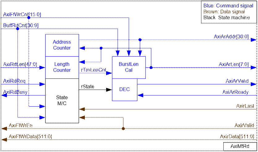
Figure 2‑14 AxiMtRd hardware
Comparing to AxiMtWr, the logic inside AxiMtRd is simpler. State machine is designed to control the sequence of command and data following AXI4 protocol. Command signal is in blue color at upper side and data signal is in brown color at lower side.
After new read request (AxiRdReq) is asserted to ‘1’, state machine changes to transfer state.
At the same time, Length counter loads total transfer size input (AxiRdLen) and Address counter is reset to 0 to prepare new transfer. Before transferring data of each burst size, state machine checks that data in DDR is enough by monitoring BuffRdCnt and free space of AxiRxFIFO is enough by monitoring AxiFfWrCnt. Then, state machine asserts read request to DDR (AxiArValid=’1’) with the valid value of DDR address (AxiArAddr) and burst size (AxiArLen).
Data from DDR is forwarded to AxiRxFIFO when AxirValid=’1’. AxirReady is fixed to ‘1’ to show ready status for receiving the data from DDR. AxirLast is monitored to check the end cycle of burst transfer.
Similar to AxiMtWr, BurstLen Cal block is designed to calculate burst size to be 512 byte, 1 kByte, 2 kByte, and 4 kByte depending on FIFO/DDR status, current address alignment, and remaining transfer size. Using bigger burst size reduces the effect of overhead time to transfer performance. Burst size is set to 4 kByte when following conditions are met.
1) Remaining transfer size is more than or equal to 4 kByte (rTrnLenCnt[47:3] is not equal to 0).
2) Current address is aligned to 4 kByte (AxiArAddr[11:0] is equal to 0).
3) BuffRdCnt value is more than or equal to 4 kByte (BuffRdCnt[30:12] is not equal to 0).
4) AxiFfWrCnt shows that at least 8 kByte free space is found (AxiFfWrCnt[15:7] is not equal to all 1).
The output of BurstLen Cal is AxiArLen signal. AxiArLen is also used to calculate the next address in Address counter and calculate remaining transfer size in Length counter.
The operation of the logic inside AxiMtRd is displayed as timing diagram in Figure 2‑15. In the example, burst size is equal to 8 for transferring 512 byte data.
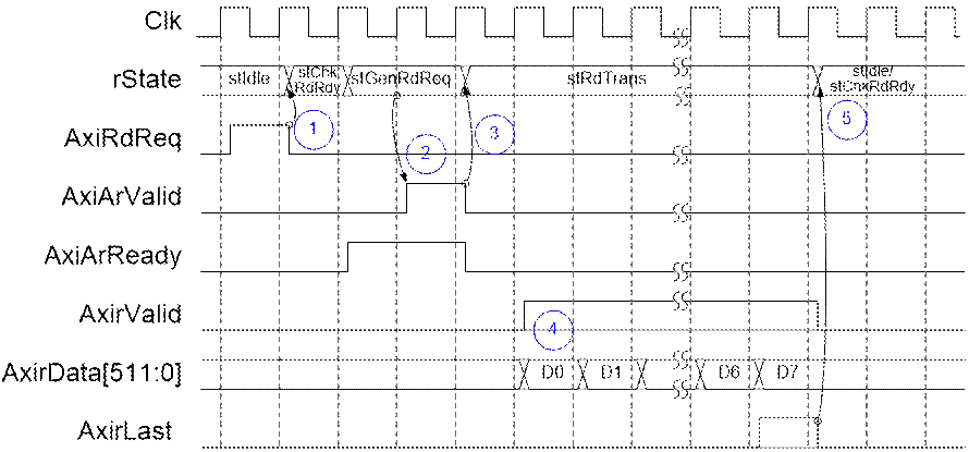
Figure 2‑15 AxiMtRd Timing diagram when burst size = 512 byte
After AxiRdReq is asserted to ‘1’, state machine changes to stChkRdRdy to monitor FIFO and DDR status. If FIFO and DDR are ready to transfer one sector data, state machine will change to next state. In stGenRdReq state, AxiArValid is asserted to ’1’ for DDR read request. After read request is received (AxiArValid=’1’ and AxiArReady=’1’), state machine changes to stRdTrans to wait 8 data from DDR. AxirValid is asserted to ‘1’ with the valid value of AxirData when DDR returns data. AxirValid and AxirData are bypassed to be FIFO write enable and FIFO write data. AxirLast is asserted to ‘1’ when transferring the last data. After transferring the last data and there is no remaining size, state machine changes from stRdTrans to stIdle. If remaining size is not zero, state machine will go back to stChkRdRdy to start new burst loop.
2.4 CPU and Peripherals
The hardware is connected to CPU through AXI4-Lite bus, similar to other CPU peripherals. The hardware registers are mapped to CPU memory address, as shown in Table 2‑2. The control and status registers for CPU access are designed in LAxi2Reg.
LAxi2Reg connects to many hardwares in the system such as DdrCtrl, TestGen, Raid0x8 and IdenRAM to get the control and status signals of each module. As shown in Figure 2‑16, there are three clock domains applied in this block, i.e. DdrClk which is used to interface with AXI4 bus of DdrCtrl, CpuClk which is used to interface with AXI4-Lite bus of CPU, and UserClk which is user clock domain for TestGen and RAID0 block.
AsyncAxiReg includes asynchronous circuit between CpuClk and UserClk while AsyncCtrl includes asynchronous circuit between DdrClk and UserClk. More details of each hardware are described as follows.
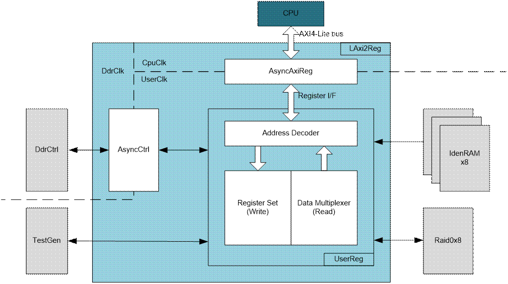
Figure 2‑16 CPU and peripherals hardware
2.4.1 AsyncCtrl
This module is designed to be asynchronous circuit of control and status signals between DdrClk and UserClk. Two register types are designed to cross clock domain. If the signal is valid only one clock cycle, latch register will be applied to latch the signal in source clock domain before transferring to destination clock domain. If the signal is stable for long time, simple D Flip-Flip will be applied for transferring signal from source clock domain to destination clock domain.
2.4.2 AsyncAxiReg
This module is designed to convert the signal interface of AXI4-Lite to be register interface. Also, it supports to convert clock domain from CpuClk to be UserClk domain. Timing diagram of register interface is shown in Figure 2‑17.
To write register, timing diagram is same as RAM interface. RegWrEn is asserted to ‘1’ with the valid signal of RegAddr (Register address in 32-bit unit), RegWrData (write data of the register), and RegWrByteEn (the byte enable of this access: bit[0] is write enable for RegWrData[7:0], bit[1] is used for RegWrData[15:8], …, and bit[3] is used for RegWrData[31:24]).
To read register, AsyncAxiReg asserts RegRdReq=’1’ with the valid value of RegAddr (the register address in 32-bit unit). After that, the module waits until RegRdValid is asserted to ‘1’ to get the read data through RegRdData signal.
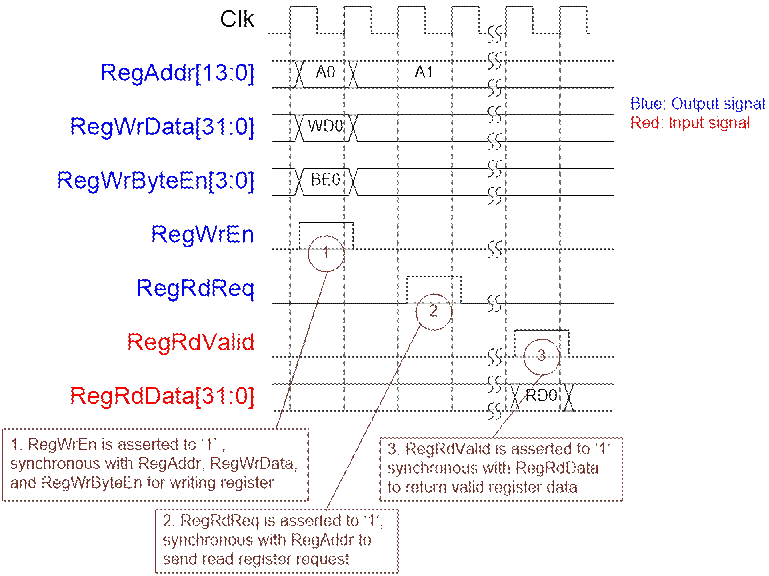
Figure 2‑17 Register interface timing diagram
2.4.3 UserReg
As shown in Figure 2‑16, after RegWrEn or RegRdReq is asserted to ‘1’ to request write or read register access, RegAddr is loaded to Address decoder to select the active register. For write register, RegWrData signal is latched to be the new value for the request register. In this module, RegWrByteEn is not used, so CPU firmware needs to access the hardware register by using 32-bit pointer only.
For read request, there are many status signals for CPU access from DdrCtrl, TestGen, Raid0x8, and IdenRAM. So, data multiplexer includes many pipelines register to select the read data to return to CPU. RegRdValid is designed by using three D Flip-flops, input by RegRdReq signal. So, the read access has three clock cycles latency after detecting RegRdReq signal.
Memory map of control and status signals inside UserReg module is shown in Table 2‑2.
Table 2‑2 Register Map
|
Address |
Register Name |
Description |
|
Rd/Wr |
(Label in the “hsataraid8ddrtest.c”) |
|
|
|
|
RAID0 block |
|
BA+0x000 |
User Address (Low) Reg |
[31:0]: Input to be start sector address (UserAddr[31:0] of dgIF typeS for RAID0) |
|
Wr |
(USRADRL_REG) |
|
|
BA+0x004 |
User Address (High) Reg |
[15:0]: Input to be start sector address (UserAddr[47:32] of dgIF typeS for RAID0) |
|
Wr |
(USRADRH_REG) |
|
|
BA+0x008 |
User Length (Low) Reg |
[31:0]: Input to be transfer length in sector unit (UserLen[31:0] of dgIF typeS for RAID0) |
|
Wr |
(USRLENL_REG) |
|
|
BA+0x00C |
User Length (High) Reg |
[15:0]: Input to be transfer length in sector unit (UserLen[47:32] of dgIF typeS for RAID0) |
|
Wr |
(USRLENH_REG) |
|
|
BA+0x010 |
User Command Reg |
[1:0]: Input to be user command (UserCmd of dgIF typeS for RAID0). “00”-Identify device, “01”-Security erase, “10”-Write Dev, “11”-Read Dev. When this register is written, the design generates command request to RAID0 to start new command operation. |
|
Wr |
(USRCMD_REG) |
|
|
BA+0x100 |
Total device size (Low) Reg |
[31:0]: Total capacity of RAID0 in sector unit (LBASize[31:0] of dgIF typeS for RAID0) |
|
Rd |
(LBASIZEL_REG) |
|
|
BA+0x104 |
Total device size (High) Reg |
[15:0]: Total capacity of RAID0 in sector unit (LBASize[47:32] of dgIF typeS for RAID0) |
|
Rd |
(LBASIZEH_REG) |
|
|
BA+0x108 |
User Status Reg |
[0]: UserBusy of dgIF typeS for RAID0 (‘0’: Idle, ‘1’: Busy) [1]: UserError of dgIF typeS for RAID0 (‘0’: Normal, ‘1’: Error) [4:3]: SATA RAID speed from IP (“00”: No linkup, “11”: SATA Gen3, Others: Not supported) [15:8]: Linkup signal, directly mapped from each SATA-IP (bit[8]-IP#0, [9]-IP#1, …, [15]-IP#7). |
|
Rd |
(USRSTS_REG) |
|
|
BA+0x110 |
User Error Type (Low) Reg |
[31:0]: User error status, directly mapped from UserErrorType[7:0] of HCTL-IP#0 - #3 (bit[7:0]: IP#0, bit[15:8]: IP#1, …, bit[31:24]: IP#3). |
|
Rd |
(USRERRTYPEL_REG) |
|
|
BA+0x114 |
User Error Type (High) Reg |
[31:0]: User error status, directly mapped from UserErrorType[7:0] of HCTL-IP#4 - #7 (bit[7:0]: IP#4, bit[15:8]: IP#5, …, bit[31:24]: IP#7). |
|
Rd |
(USRERRTYPEH_REG) |
|
|
BA+0x120 |
Test pin of SATA HCTL-IP#0 Reg |
[31:0]: TestPin[0][31:0] of RAID0x8 which is direct mapped from TestPin of SATA HCTL-IP#0 |
|
Rd |
(TESTPIN0_REG) |
|
|
BA+0x124 |
Test pin of SATA HCTL-IP#1 Reg |
[31:0]: TestPin[1][31:0] of RAID0x8 which is direct mapped from TestPin of SATA HCTL-IP#1 |
|
Rd |
(TESTPIN1_REG) |
|
|
BA+0x128 |
Test pin of SATA HCTL-IP#2 Reg |
[31:0]: TestPin[2][31:0] of RAID0x8 which is direct mapped from TestPin of SATA HCTL-IP#2 |
|
Rd |
(TESTPIN2_REG) |
|
|
BA+0x12C |
Test pin of SATA HCTL-IP#3 Reg |
[31:0]: TestPin[3][31:0] of RAID0x8 which is direct mapped from TestPin of SATA HCTL-IP#3 |
|
Rd |
(TESTPIN3_REG) |
|
|
BA+0x130 |
Test pin of SATA HCTL-IP#4 Reg |
[31:0]: TestPin[4][31:0] of RAID0x8 which is direct mapped from TestPin of SATA HCTL-IP#4 |
|
Rd |
(TESTPIN4_REG) |
|
|
BA+0x134 |
Test pin of SATA HCTL-IP#5 Reg |
[31:0]: TestPin[5][31:0] of RAID0x8 which is direct mapped from TestPin of SATA HCTL-IP#5 |
|
Rd |
(TESTPIN5_REG) |
|
|
BA+0x138 |
Test pin of SATA HCTL-IP#6 Reg |
[31:0]: TestPin[6][31:0] of RAID0x8 which is direct mapped from TestPin of SATA HCTL-IP#6 |
|
Rd |
(TESTPIN6_REG) |
|
|
BA+0x13C |
Test pin of SATA HCTL-IP#7 Reg |
[31:0]: TestPin[7][31:0] of RAID0x8 which is direct mapped from TestPin of SATA HCTL-IP#7 |
|
Rd |
(TESTPIN7_REG) |
Address |
Register Name |
Description |
|
Rd/Wr |
(Label in the “hsataraid8ddrtest.c”) |
|
|
|
|
TestGen block |
|
BA+0x200 |
Test Pattern Reg |
[2:0]: Test pattern select “000”-Increment, “001”-Decrement, “010”-All 0, “011”-All 1, “100”-LFSR |
|
Wr |
(PATTSEL_REG) |
|
|
BA+0x204 |
Transfer Ratio Reg |
Set the sustain rate for write or read access of TestGen module. [11:8]: the numerator of the ratio, [3:0]: the denominator of the ratio. Transfer Rate (bit/sec) = (Numerator/Denominator) x UserClk (200MHz) x 256-bit |
|
Wr |
(TRNRATIO_REG) |
|
|
BA+0x208 |
DDR Read threshold |
[11:0]: The threshold value of DDR buffer in MB unit. TestGen module waits until the data in DDR is more than or equal to the threshold value before start reading the 1st data from DDR as sustain rate when user sends Read command (USRCMD_REG=”11”). Valid range is 0-4095 MB. |
|
Wr |
(DDRRDTHR_REG) |
|
|
BA+0x300 |
TestGen status |
[0]: Busy flag of write operation from TestGen. (‘0’: No operation, ‘1’: Write is operating). [1]: Busy flag of read operation from TestGen (‘0’: No operation, ‘1’: Read is operation). Note that this flag is asserted after data in DDR is equal or more than threshold value, set by DDRRDTHR_REG. [2]: Busy flag of write operation from DdrCtrl (‘0’: No operation, ‘1’: Write is operating). [3]: Busy flag of read operation from DdrCtrl (‘0’: No operation, ‘1’: Write is operating). [4]: Verification Fail (‘0’: Normal, ‘1’: Data verification is failed) [5]: Error from buffer overflow during Write command (‘0’: Normal, ‘1’: AxiTxFIFO is full during sustain write) [6]: Error from buffer underflow during Read command (‘0’: Normal, ‘1’: AxiRxFIFO is empty during sustain read) |
|
Rd |
PATTSTS_REG |
|
|
BA+0x320 |
Expected value Word0 Reg |
[31:0]: Latch value of expected data [31:0] in TestGen during Read command |
|
Rd |
(EXPPATW0_REG) |
|
|
BA+0x324 |
Expected value Word1 Reg |
[31:0]: Latch value of expected data [63:32] in TestGen during Read command |
|
Rd |
(EXPPATW1_REG) |
|
|
BA+0x328 |
Expected value Word2 Reg |
[31:0]: Latch value of expected data [95:64] in TestGen during Read command |
|
Rd |
(EXPPATW2_REG) |
|
|
BA+0x32C |
Expected value Word3 Reg |
[31:0]: Latch value of expected data [127:96] in TestGen during Read command |
|
Rd |
(EXPPATW3_REG) |
|
|
BA+0x330 |
Expected value Word4 Reg |
[31:0]: Latch value of expected data [159:128] in TestGen during Read command |
|
Rd |
(EXPPATW4_REG) |
|
|
BA+0x334 |
Expected value Word5 Reg |
[31:0]: Latch value of expected data [191:160] in TestGen during Read command |
|
Rd |
(EXPPATW5_REG) |
|
|
BA+0x338 |
Expected value Word6 Reg |
[31:0]: Latch value of expected data [223:192] in TestGen during Read command |
|
Rd |
(EXPPATW6_REG) |
|
|
BA+0x33C |
Expected value Word7 Reg |
[31:0]: Latch value of expected data [255:224] in TestGen during Read command |
|
Rd |
(EXPPATW7_REG) |
|
|
BA+0x340 |
Read value Word0 Reg |
[31:0]: Latch value of read data [31:0] in TestGen during Read command |
|
Rd |
(RDPATW0_REG) |
|
|
BA+0x344 |
Read value Word1 Reg |
[31:0]: Latch value of read data [63:32] in TestGen during Read command |
|
Rd |
(RDPATW1_REG) |
|
|
BA+0x348 |
Read value Word2 Reg |
[31:0]: Latch value of read data [95:64] in TestGen during Read command |
|
Rd |
(RDPATW2_REG) |
|
|
BA+0x34C |
Read value Word3 Reg |
[31:0]: Latch value of read data [127:96] in TestGen during Read command |
|
Rd |
(RDPATW3_REG) |
|
|
BA+0x350 |
Read value Word0 Reg |
[31:0]: Latch value of read data [159:128] in TestGen during Read command |
|
Rd |
(RDPATW4_REG) |
|
|
BA+0x354 |
Read value Word1 Reg |
[31:0]: Latch value of read data [191:160] in TestGen during Read command |
|
Rd |
(RDPATW5_REG) |
Address |
Register Name |
Description |
|
Rd/Wr |
(Label in the “hsataraid8ddrtest.c”) |
|
|
BA+0x358 |
Read value Word2 Reg |
[31:0]: Latch value of read data [223:192] in TestGen during Read command |
|
Rd |
(RDPATW6_REG) |
|
|
BA+0x35C |
Read value Word3 Reg |
[31:0]: Latch value of read data [255:224] in TestGen during Read command |
|
Rd |
(RDPATW7_REG) |
|
|
BA+0x360 |
Data Failure Address (Low)Reg |
[31:0]: Latch value of failure address [31:0] in byte unit from Read command |
|
Rd |
(RDFAILNOL_REG) |
|
|
BA+0x364 |
Data Failure Address (High)Reg |
[24:0]: Latch value of failure address [56:32] in byte unit from Read command |
|
Rd |
(RDFAILNOH_REG) |
|
|
BA+0x368 |
Current test byte (Low) Reg |
[31:0]: Current test data size of TestGen module in byte unit (bit[31:0]) |
|
Rd |
(CURTESTSIZEL_REG) |
|
|
BA+0x36C |
Current test byte (High) Reg |
[24:0]: Current test data size of TestGen module in byte unit (bit[56:32]) |
|
Rd |
(CURTESTSIZEH_REG) |
|
|
BA+0x370 |
DDR Write Address Reg |
[31:0]: Current DDR write address in byte unit (bit[8:0] is fixed to 0 to align 512-byte unit) |
|
Rd |
(DDRWRADDR_REG) |
|
|
BA+0x374 |
DDR Read Address Reg |
[31:0]: Current DDR read address in byte unit (bit[8:0] is fixed to 0 to align 512-byte unit) |
|
Rd |
(DDRRDADDR_REG) |
|
|
Identify device RAM |
||
|
BA+0x2000 – 0x21FF |
Identify Device Command Data (IDENCTRL0_REG) |
512-byte Identify device data from SATA CH#0 |
|
BA+0x2200 – 0x23FF |
Identify Device Command Data (IDENCTRL1_REG) |
512-byte Identify device data from SATA CH#1 |
|
BA+0x2400 – 0x25FF |
Identify Device Command Data (IDENCTRL2_REG) |
512-byte Identify device data from SATA CH#2 |
|
BA+0x2600 – 0x27FF |
Identify Device Command Data (IDENCTRL3_REG) |
512-byte Identify device data from SATA CH#3
|
|
BA+0x2800 – 0x29FF |
Identify Device Command Data (IDENCTRL4_REG) |
512-byte Identify device data from SATA CH#4
|
|
BA+0x3000 – 0x31FF |
Identify Device Command Data (IDENCTRL5_REG) |
512-byte Identify device data from SATA CH#5
|
|
BA+0x3200 – 0x33FF |
Identify Device Command Data (IDENCTRL6_REG) |
512-byte Identify device data from SATA CH#6
|
|
BA+0x3400 – 0x35FF |
Identify Device Command Data (IDENCTRL7_REG) |
512-byte Identify device data from SATA CH#7
|
3 CPU Firmware
After system boot-up, CPU initializes its peripherals such as UART and Timer. Next, CPU monitors link up signal of all SATA devices by comparing USRSTS_REG[15:8]=0xFF. Main menu is displayed after all SATA devices link up.
CPU firmware supports four commands, following USRCMD_REG value, i.e. “00” for Identify device, “01” for Security erase, “10” for Write, and “11” for Read. More details of the sequence in each command are described as follows.
3.1 Identify device command
The sequence of the firmware when user selects Identify device command is below.
1) Set USRCMD_REG=”00”. Next, RAID0 sends Identify device command to all SATA HCTL-IPs. RAID0 busy flag (USRSTS_REG[0]) changes from ‘0’ to ‘1’.
2) CPU waits until the operation is completed or some errors are found by monitoring USRSTS_REG value. Bit[0] is de-asserted to ‘0’ when command is completed. Bit[1] is asserted to ‘1’ when some errors are detected. In case of error condition, there is error message displayed on the console. If the command is completed, the data from Identify device command of all SATA devices will be stored in IdenRAMs.
3) CPU reads Identify device data from IdenRAMs which are mapped to IDENCTRL0_REG – IDENCTRL1_REG7 address. Then, CPU displays the information such as SATA device model name, security feature set supported, and erase time value on Serial console. Also, RAID0 device capacity (LBASIZEL/H_REG) is displayed in GB unit on the console.
3.2 Write/Read command
The sequence of the firmware when user selects Write/Read command is below.
1) Receive start address, transfer length, test pattern, sustain rate, DDR threshold value from user through Serial console. If some inputs are invalid, the operation will be cancelled.
2) Get all inputs and set the value to USRADRL/H_REG, USRLENL/H_REG, TRNRATIO_REG, DDRRDTHR_REG, PATTSEL_REG, and USRCMD_REG (USRCMD_REG=”10” for write transfer, and “11” for read transfer).
3) CPU waits until the operation is completed or some errors (except verification error) are found by monitoring USRSTS_REG[1:0] and PATTSTS_REG[6:0]. PATTSTS_REG[3:0] is monitored because CPU needs to wait until PattGen module completes to verify all data from DDR in Read command.
If some bits of PATTSTS_REG[6:5] (buffer overflow/underflow flag) are asserted to ‘1’, the operation will be cancelled with displaying error message. Next, CPU waits for 10 sec which is SATA-HCTL timeout value and reads USRSTS_REG[1] to show RAID0 error status. The error from RAID0 can be caused to buffer overflow and underflow error.
If PATTSTS_REG[4] is asserted to ‘1’, verification error message will be displayed. After that, CPU still runs until end of operation or user inputs any key.
4) During running command, current transfer size reading from CURTESTSIZE_REG is displayed every second. Finally, test performance is displayed on Serial console when command is completed.
3.3 Security erase command
The sequence of the firmware when user selects Security erase command is below.
1) Set USRCMD_REG=”01”. Next, RAID0 sends Security erase command to all SATA HCTL-IPs. RAID0 busy flag (USRSTS_REG[0]) changes from ‘0’ to ‘1’.
2) CPU waits until command complete by monitoring USRSTS_REG value. Bit[0] is de-asserted to ‘0’ when command is completed. This operation may use long time to operate, so there is dummy message displayed on the console every second to show system alive status. Finally, total time usage is displayed on Serial console when command is completed.
4 Example Test Result
The example test result when running demo system by using 8x1 TB Samsung 850 Pro is shown in Figure 4‑1.
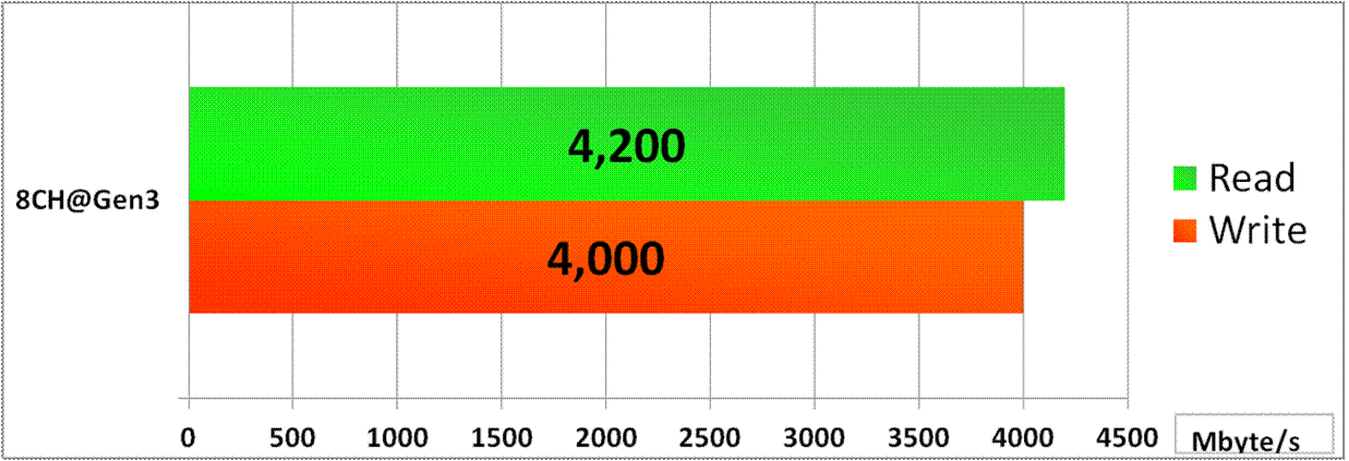
Figure 4‑1 Test Performance of RAID0x8 IP demo by using Samsung 850 Pro SSD
When running 8-ch RAID0 with 8 SATA Gen3 SSDs on KCU105 board, write sustain performance is about 4,000 Mbyte/sec and read sustain performance is about 4,200 Mbyte/sec.
5 Revision History
|
Revision |
Date |
Description |
|
1.0 |
13-Mar-18 |
Initial version release |
Copyright: 2018 Design Gateway Co,Ltd.