System Architecture
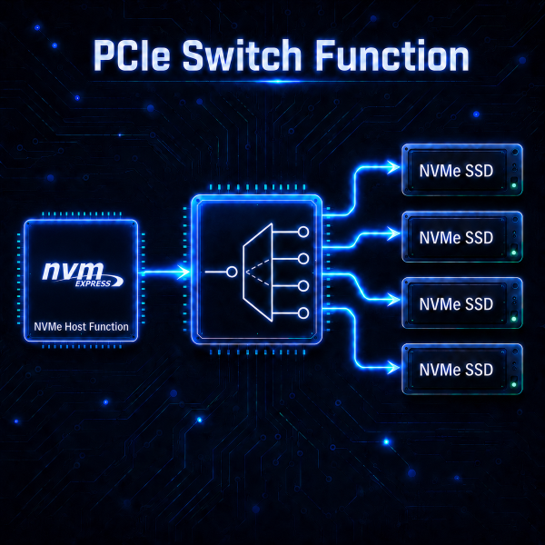
NVMeSW-IP Connectivity
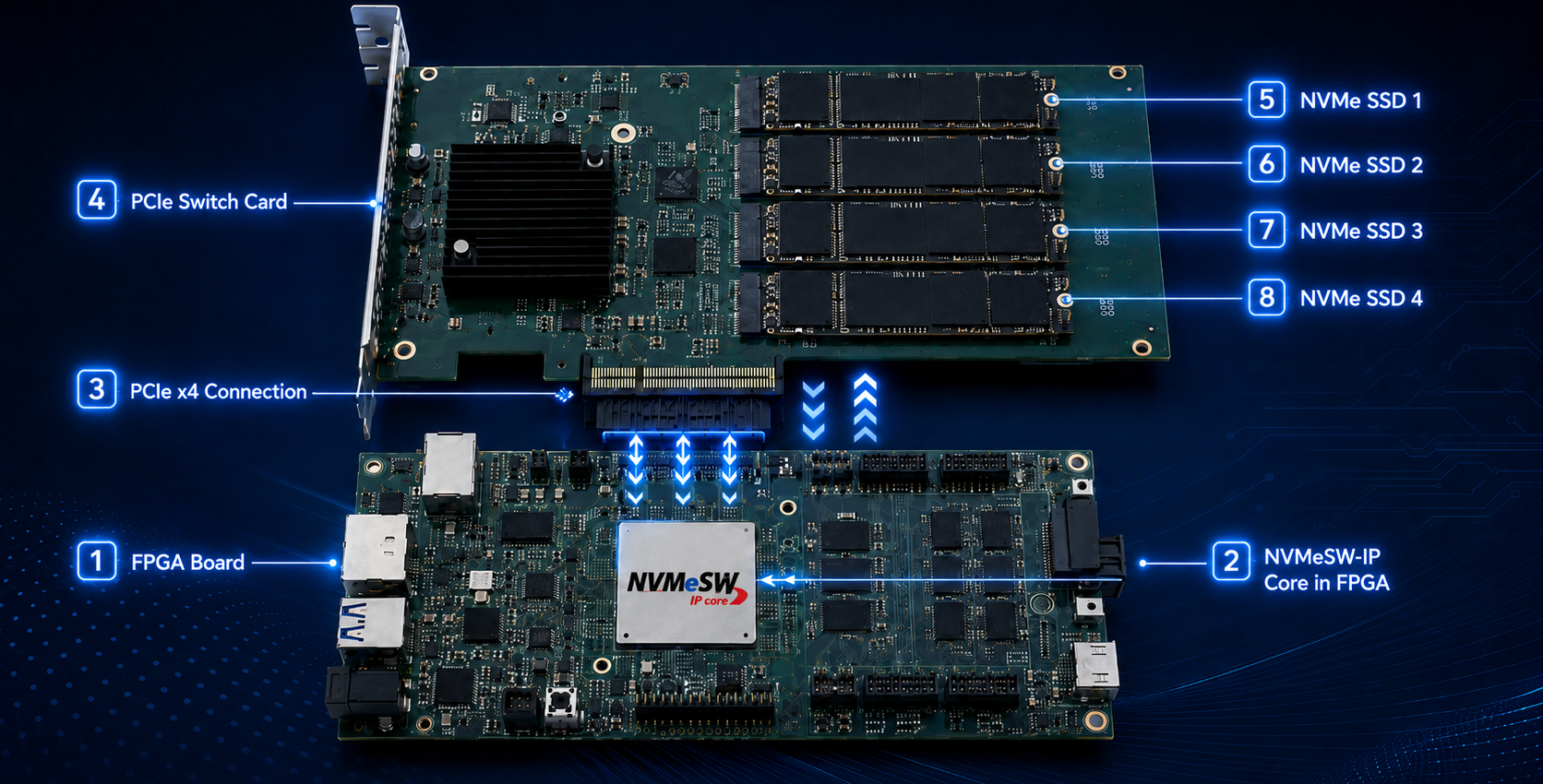
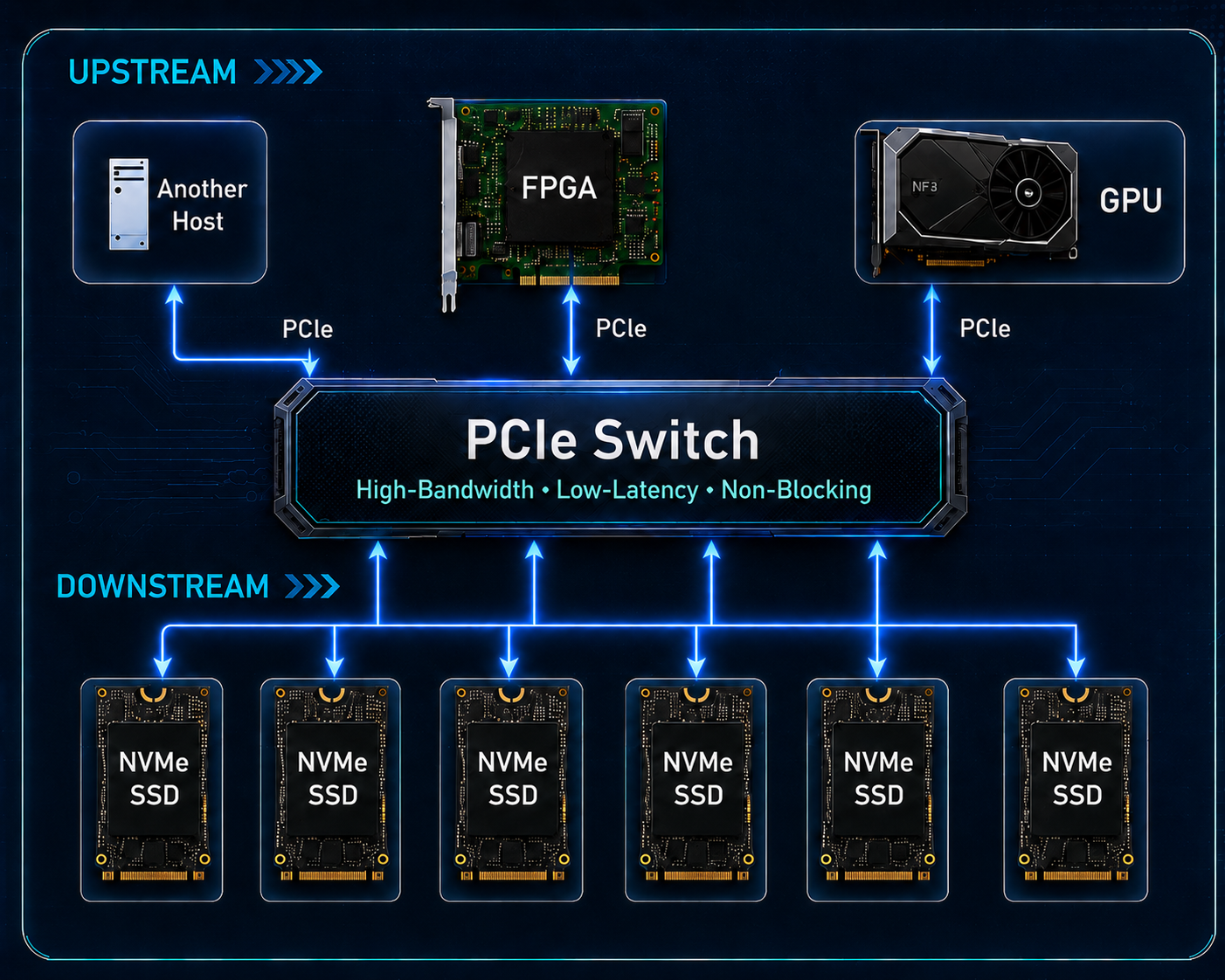
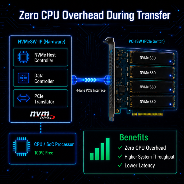
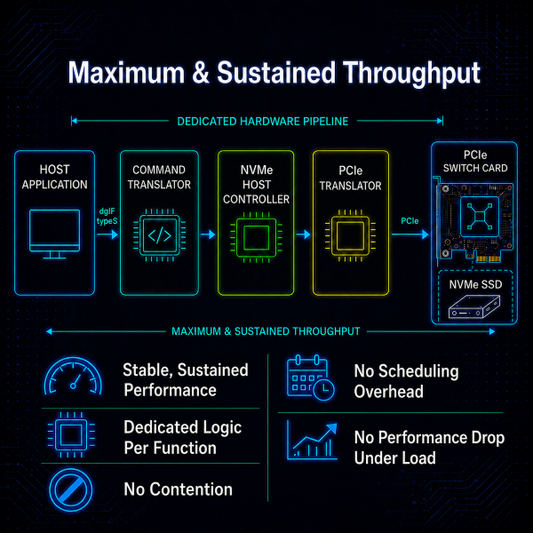
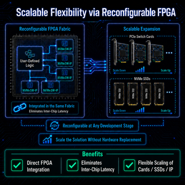
A fully hardware-based FPGA solution that enables simultaneous, high-bandwidth access to multiple NVMe SSDs through a PCIe switch fabric — with no CPU cycles consumed during data transfer, no DDR buffer required, and deterministic wire-speed performance from the first byte to the last.
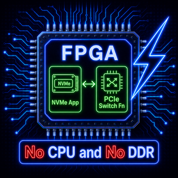
General-purpose CPU-based NVMe drivers are not designed for deterministic, high-throughput, multi-drive scenarios. FPGA-based NVMe control unlocks capabilities that no software stack can match.
The combination of deterministic timing, high bandwidth, and rugged FPGA deployment makes NVMeSW-IP particularly well-suited for demanding sectors.
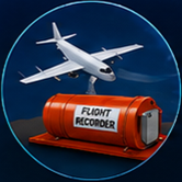
No-Gap Lossless Write — Continuous lossless write of avionics, video, and flight data to multiple NVMe SSDs with zero recording gaps. FPGA controls high-speed writes; an external host retrieves or reconfigures data post-mission.
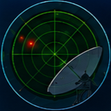
Wideband Data Capture at Multi-GB/s Rates — Multi-GB/s wideband RF capture striped across SSDs. FPGA performs real-time filtering; GPU/SoC runs target detection, spectrum analysis, or EW classification.

Downlink Buffering and Retransmission — Camera, sensor, and comm data buffered to NVMe arrays before downlink. FPGA manages high-speed storage; SoC/GPU handles compression, encryption, and packetization.
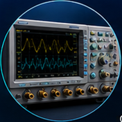
Gapless Capture for Oscilloscopes and Digitizers — NVMeSW-IP streams samples directly from FPGA logic to multiple NVMe SSDs for gapless, long-duration recording — no lost transients, no large memory buffers required.
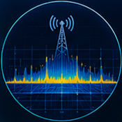
Wideband Streaming for Spectrum and Protocol Test — Wideband RF and I/Q data is recorded to NVMe SSD arrays at multi-GB/s rates. FPGA handles real-time preprocessing; GPU or SoC performs spectrum analysis, modulation analysis, or anomaly detection.
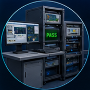
Large Test-Data Buffering, Replay and Post-Analysis — Multiple NVMe SSDs form a scalable high-speed buffer; FPGA executes deterministic test transfers, while a host manages device programming, test flow, and result collection.
| FPGA Development Kit |
AMD
— KCU105, ZCU106, VCU118 Altera — Arria 10 GX Development Kit |
| PCIe Switch Card | Quattro 400 M.2 NVMe SSD Adapter | Squid SKU-086-34 NVMe SSD Adapter |
| NVMe SSDs | NVMe PCIe SSDs (Gen3) |
| Host PC | Windows or Linux PC for initial programming and monitoring via UART / JTAG |
| IP Core | NVMeSW-IP (NVMe IP Core for PCIe Switch) |
| Reference Design | NVMeSW-IP Reference Design |
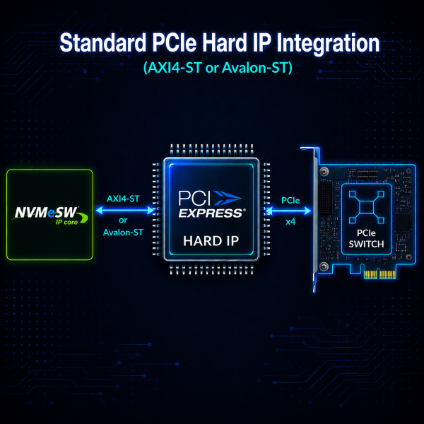
NVMeSW-IP for AMD FPGAs (KCU105, ZCU106, VCU118). Supports AXI4-ST interface to PCIe Hard IP. A free evaluation demo for AMD KCU105 is publicly available.
| AMD (KCU105) | Download ↓ |
NVMeSW-IP for Altera FPGAs (Arria 10 GX). Supports Avalon-ST interface to PCIe Hard IP. A free evaluation demo for Arria 10 GX is publicly available.
| Altera (A10GX) | Download ↓ |