Design Gateway — Special Reference Design

Sustained-Rate Data Logging & Monitoring
with NVMe-IP + DDR Memory Buffer

Special Reference Design  for  Stable Continuous Write to NVMe SSD via FPGA
NVMe-IP Core DDR Buffer No CPU / No OS Sustained Rate AMD KCU105
2,800
MB/s
Sustained Write

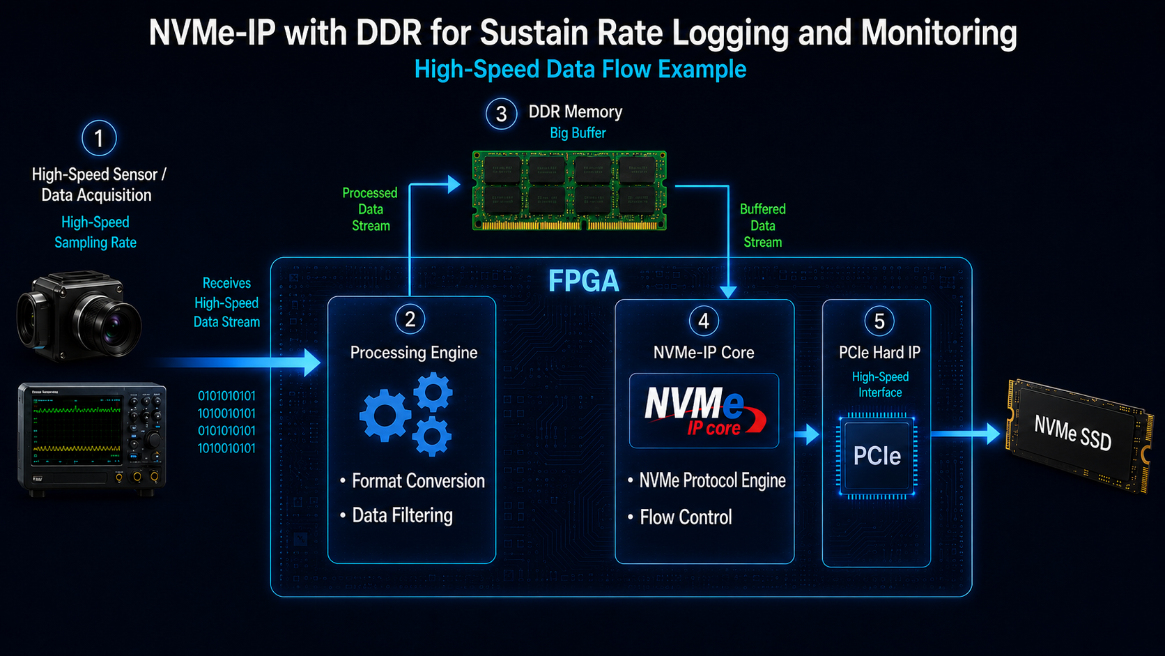
A fully hardware-based FPGA solution that delivers stable, continuous write throughput to NVMe SSD at multi-GB/s speeds — absorbing SSD write-speed variations via an external DDR buffer with no CPU or OS required.

System Architecture
High-Speed Data Flow
NVMe-IP DDR Data Flow Diagram
The Challenge
Consumer SSDs vs Enterprise SSDs

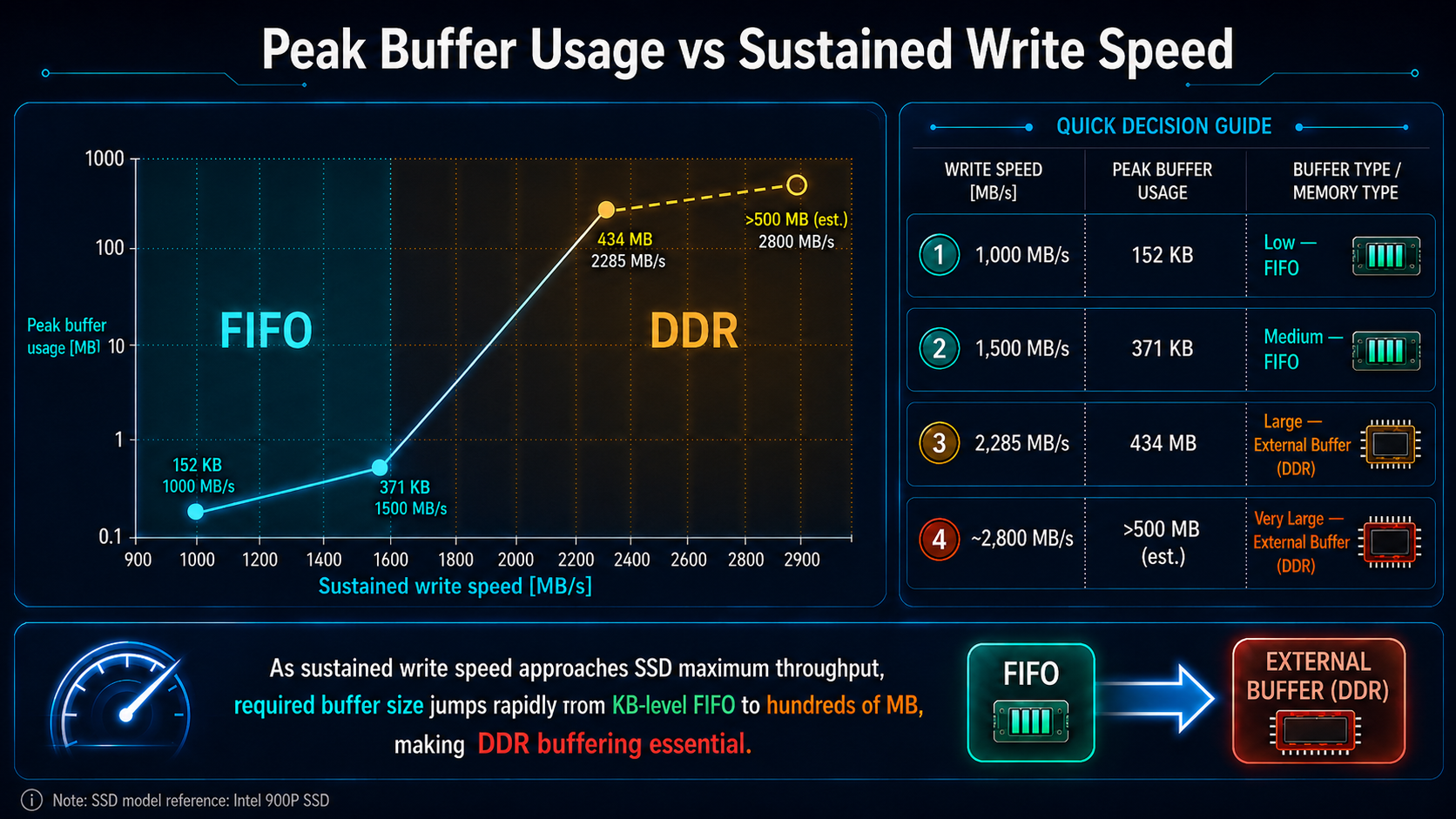
Not all NVMe SSDs behave the same under sustained write workloads. Consumer SSDs maximize peak benchmark numbers using write-cache techniques, while enterprise SSDs are built for predictable continuous throughput. Understanding this difference is critical when selecting storage for applications requiring a guaranteed sustained data rate.

SSD Type
Consumer SSDs
High Burst Performance
Deliver impressive peak write speeds via SLC write-cache regions. Benchmarks show multi-GB/s throughput, but only for short bursts before the cache saturates.
Performance Drops Under Sustained Workloads
Once the write cache is exhausted, throughput collapses to a fraction of advertised peak and fluctuates unpredictably — unsuitable for real-time applications.
Designed for Consumer Use
Optimized for bursty desktop workloads — gaming, boot times, general OS use. Not validated for continuous high-throughput industrial or mission-critical applications.
SSD Type
Enterprise SSDs
Consistent Performance
Maintain stable, predictable throughput from the first byte to the last, regardless of drive fill level or workload duration. QoS guarantees ensure tight latency and bandwidth bounds.
Optimized for Sustained Write Workloads
Advanced wear-leveling, larger over-provisioning, and high-endurance NAND handle continuous sequential write operations hour after hour without throughput degradation.
Built for Enterprise Reliability
Rated for high DWPD multiples with power-loss protection, end-to-end data integrity, and validated MTBF suited for 24/7 mission-critical deployments.
System Design
Key Features — NVMe SSD Characteristic Test Platform
NVMe SSD Characteristic Test Platform
▸ Input
Configurable
Configurable DDR Buffer Size
Adjust buffer capacity to absorb SSD throughput fluctuations during sustained-rate testing. Users set and tune the DDR allocation per run, sizing the buffer precisely to the required sustained write speed without over-provisioning.
Parametric
Write / Read Test Speed
Set the target write and read rates to evaluate sustained SSD performance. The system drives data at the configured speed continuously, revealing the true sustained throughput capability of any NVMe SSD under test conditions.
▸ Output
Result
Pass / Fail Result
Shows whether the NVMe SSD passes the sustained-rate write/read test conditions. A clear pass/fail indicator lets engineers quickly determine if the drive meets the throughput requirements of the target application.
Measurement
Maximum DDR Buffer Usage
Displays the peak DDR buffer utilization reached during the test. This metric reveals the minimum DDR capacity required for a given sustained write speed, allowing right-sizing of the external DDR for the specific application.
Measured Results
Performance Results

Evaluated on the AMD KCU105 FPGA board with a Design Gateway AB18-PCIeX16 adapter and Intel 900P Optane SSD. A 280 GB LFSR pattern was written at each target speed; peak DDR buffer occupancy was recorded per run.

Peak Buffer Usage vs Sustained Write Speed
Analysis: DDR buffer demand scales with sustained write speed — and crosses a critical threshold between 1,500 MB/s and 2,285 MB/s, where usage jumps from KB-range to hundreds of MB. Below this threshold, an FPGA internal FIFO suffices. Above it, external DDR becomes mandatory. This test platform measures that threshold directly, giving engineers the empirical data needed to select the right SSD and size the DDR with confidence before committing to hardware.
Technical Specs
System Requirements
FPGA Development KitAMD KCU105 Evaluation Kit
SSD Interface AdapterDesign Gateway AB18-PCIeX16  |  AB17-M2FMC
NVMe SSDIntel 900P Optane NVMe SSD
IP CoreNVMe-IP Core with DDR Reference Design
Reference DesignNVMe-IP DDR Reference Design for Sustained Data Rate
Live Demonstration
Start Your Free Evaluation

A free evaluation demo for the AMD KCU105 is publicly available, allowing you to directly verify sustained-rate NVMe write performance — including peak DDR buffer usage — on real hardware.

For more details, please refer to the demo video and documentation published on our website.

📄 Reference Design Document 📋 Demo Instruction Manual 🔗 NVMe-IP Core Product Page
💾 Free Evaluation Demo
ConfigurationFPGA BoardAdapterDownload
KCU105 + AB17AMD KCU105AB17-M2FMCDownload ↓
KCU105 + AB18AMD KCU105AB18-PCIeX16Download ↓
DEMO VIDEO
NVMe-IP DDR Reference Design
Sustained Data Rate Demo on Xilinx KCU105
▶ Watch Demo Video
■ For a time-limited free demo evaluation, please contact us